EFM32G200F64 Energy Micro, EFM32G200F64 Datasheet - Page 17
EFM32G200F64
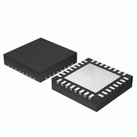
Manufacturer Part Number
EFM32G200F64
Description
MCU 32BIT 64KB FLASH 32-QFN
Manufacturer
Energy Micro
Series
Geckor
Datasheets
1.EFM32G200F16.pdf
(63 pages)
2.EFM32G200F16.pdf
(10 pages)
3.EFM32G200F16.pdf
(463 pages)
4.EFM32G200F16.pdf
(136 pages)
Specifications of EFM32G200F64
Core Processor
ARM® Cortex-M3™
Core Size
32-Bit
Speed
32MHz
Connectivity
EBI/EMI, I²C, IrDA, SmartCard, SPI, UART/USART
Peripherals
Brown-out Detect/Reset, DMA, POR, PWM, WDT
Number Of I /o
24
Program Memory Size
64KB (64K x 8)
Program Memory Type
FLASH
Ram Size
16K x 8
Voltage - Supply (vcc/vdd)
1.8 V ~ 3.8 V
Data Converters
A/D 4x12b, D/A 1x12b
Oscillator Type
External
Operating Temperature
-40°C ~ 85°C
Package / Case
32-VQFN Exposed Pad
Processor Series
EFM32G200
Core
ARM Cortex-M3
Data Bus Width
32 bit
Data Ram Size
16 KB
Interface Type
I2C, UART
Maximum Clock Frequency
32 MHz
Number Of Programmable I/os
24
Number Of Timers
2
Operating Supply Voltage
1.8 V to 3.8 V
Maximum Operating Temperature
+ 85 C
Mounting Style
SMD/SMT
Minimum Operating Temperature
- 40 C
Lead Free Status / RoHS Status
Lead free / RoHS Compliant
Eeprom Size
-
Lead Free Status / Rohs Status
Details
Available stocks
Company
Part Number
Manufacturer
Quantity
Price


2.2.4 Software ordering of memory accesses
2011-02-04 - d0002_Rev1.00
1
The Code, SRAM, and external RAM regions can hold programs. However, ARM recommends that
programs always use the Code region. This is because the processor has separate buses that enable
instruction fetches and data accesses to occur simultaneously.
The MPU can override the default memory access behavior described in this section. For more
information, see Section 4.5 (p. 113) .
The order of instructions in the program flow does not always guarantee the order of the corresponding
memory transactions. This is because:
• the processor can reorder some memory accesses to improve efficiency, providing this does not affect
• the processor has multiple bus interfaces
• memory or devices in the memory map have different wait states
• some memory accesses are buffered or speculative.
Section 2.2.2 (p. 16) describes the cases where the memory system guarantees the order of memory
accesses. Otherwise, if the order of memory accesses is critical, software must include memory barrier
instructions to force that ordering. The processor provides the following memory barrier instructions:
DMB
DSB
ISB
Use memory barrier instructions in, for example:
• MPU programming:
• Vector table. If the program changes an entry in the vector table, and then enables the corresponding
See Section 2.2.1 (p. 15) for more information.
Address
range
0x60000000-
0x9FFFFFFF
0xA0000000-
0xDFFFFFFF
0xE0000000-
0xE00FFFFF
0xE0100000-
0xFFFFFFFF
the behavior of the instruction sequence.
• Use a DSB instruction to ensure the effect of the MPU takes place immediately at the end of context
• Use an ISB instruction to ensure the new MPU setting takes effect immediately after programming
exception, use a DMB instruction between the operations. This ensures that if the exception is taken
immediately after being enabled the processor uses the new exception vector.
switching.
the MPU region or regions, if the MPU configuration code was accessed using a branch or call.
If the MPU configuration code is entered using exception mechanisms, then an ISB instruction is
not required.
Memory region
External RAM
External device
Private
Peripheral Bus
Reserved
Memory
type
Normal
Device
Strongly-
ordered
Device
1
1
1
1
The Data Memory Barrier (DMB) instruction ensures that
outstanding memory transactions complete before subsequent
memory transactions. See Section 3.10.3 (p. 81) .
The Data Synchronization Barrier (DSB) instruction ensures that
outstanding memory transactions complete before subsequent
instructions execute. See Section 3.10.4 (p. 82) .
The Instruction Synchronization Barrier (ISB) ensures that the effect
of all completed memory transactions is recognizable by subsequent
instructions. See Section 3.10.5 (p. 82) .
XN
-
XN
XN
XN
1
1
1
Description
Executable region for data.
External Device memory
This region includes the NVIC, System timer, and system control
block.
Reserved
...the world's most energy friendly microcontrollers
17
www.energymicro.com
Related parts for EFM32G200F64
Image
Part Number
Description
Manufacturer
Datasheet
Request
R

Part Number:
Description:
KIT STARTER EFM32 GECKO
Manufacturer:
Energy Micro
Datasheet:

Part Number:
Description:
KIT DEV EFM32 GECKO LCD SUPPORT
Manufacturer:
Energy Micro
Datasheet:

Part Number:
Description:
BOARD PROTOTYPING FOR EFM32
Manufacturer:
Energy Micro
Datasheet:

Part Number:
Description:
KIT DEVELOPMENT EFM32 GECKO
Manufacturer:
Energy Micro
Datasheet:

Part Number:
Description:
MCU, MPU & DSP Development Tools TG840 Sample Kit
Manufacturer:
Energy Micro
Datasheet:

Part Number:
Description:
MCU, MPU & DSP Development Tools TG Starter Kit
Manufacturer:
Energy Micro
Datasheet:
Part Number:
Description:
MCU, MPU & DSP Development Tools TG108 Sample Kit
Manufacturer:
Energy Micro
Part Number:
Description:
MCU, MPU & DSP Development Tools TG210 Sample Kit
Manufacturer:
Energy Micro
Datasheet:
Part Number:
Description:
MCU, MPU & DSP Development Tools TG822 Sample Kit
Manufacturer:
Energy Micro
Datasheet:
Part Number:
Description:
MCU, MPU & DSP Development Tools TG230 Sample Kit
Manufacturer:
Energy Micro

Part Number:
Description:
SAMPLE KIT (SMALL BOX - CONTAINING 2 DEVICES)
Manufacturer:
Energy Micro
Part Number:
Description:
SAMPLE KIT (SMALL BOX - CONTAINING 2 DEVICES)
Manufacturer:
Energy Micro