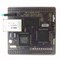
EZ80F920120MOD Zilog, EZ80F920120MOD Datasheet - Page 82

EZ80F920120MOD
Manufacturer Part Number
EZ80F920120MOD
Description
MODULE EZ80F92 512K 20MHZ
Manufacturer
Zilog
Datasheets
1.EZ80F920120MOD.pdf
(269 pages)
2.EZ80F920120MOD.pdf
(4 pages)
3.EZ80F920120MOD.pdf
(2 pages)
Specifications of EZ80F920120MOD
Module/board Type
Development Module
Processor Series
EZ80F92x
Core
eZ80
Data Bus Width
8 bit
Program Memory Type
Flash
Program Memory Size
1 MB
Interface Type
Cable
Maximum Clock Frequency
20 MHz
Operating Supply Voltage
0 V to 3.3 V
Maximum Operating Temperature
+ 70 C
Mounting Style
SMD/SMT
Package / Case
LQFP
Development Tools By Supplier
eZ80F920200ZCOG
Minimum Operating Temperature
0 C
For Use With/related Products
eZ80F92
Lead Free Status / RoHS Status
Contains lead / RoHS non-compliant
Other names
269-3157
EZ80F920120MOD
EZ80F920120MOD
- Current page: 82 of 269
- Download datasheet (4Mb)
PS015308-0404
Chip Select x Upper Bound Register
For Memory Chip Selects, the Chip Select x Upper Bound registers, detailed in Chip
Select x Upper Bound Register (CS0_UBR = 00A9h, CS1_UBR = 00ACh, CS2_UBR =
corresponding Chip Select (if enabled) can be active. For I/O Chip Selects, this register
produces no effect. The reset state for the Chip Select 0 Upper Bound register is
while the reset state for the other Chip Select upper bound registers is
Table 23. Chip Select x Upper Bound Register
(CS0_UBR = 00A9h, CS1_UBR = 00ACh, CS2_UBR = 00AFh, CS3_UBR = 00B2h)
Chip Select x Control Register
The Chip Select x Control register, detailed in Chip Select x Control Register (CS0_CTL
= 00AAh, CS1_CTL = 00ADh, CS2_CTL = 00B0h, CS3_CTL = 00B3h), enables the
Chip Selects, specifies the type of Chip Select, and sets the number of WAIT states. The
reset state for the Chip Select 0 Control register is
Chip Select control registers is
00AFh, CS3_UBR = 00B2h), defines the upper bound of the address range for which the
Bit
CS0_UBR Reset
CS1_UBR Reset
CS2_UBR Reset
CS3_UBR Reset
CPU Access
Note: R/W = Read/Write.
Bit
Position
[7:0]
CSx_UBR
Value Description
00h–
FFh
R/W
For Memory Chip Selects (
This byte specifies the upper bound of the Chip Select
address range. The upper byte of the address bus,
ADDR[23:16], is compared to the values contained in these
registers for determining whether a Chip Select signal should
be generated.
For I/O Chip Selects (CSx_IO = 1)
No effect.
P R E L I M I N A R Y
7
1
0
0
0
00h
R/W
.
6
1
0
0
0
R/W
5
1
0
0
0
E8h
R/W
4
1
0
0
0
, while the reset state for the 3 other
CSX_IO
R/W
3
1
0
0
0
Chip Selects and Wait States
Product Specification
= 0)
R/W
2
1
0
0
0
eZ80F92/eZ80F93
00h
.
R/W
1
1
0
0
0
FFh
R/W
,
0
1
0
0
0
70
Related parts for EZ80F920120MOD
Image
Part Number
Description
Manufacturer
Datasheet
Request
R

Part Number:
Description:
Communication Controllers, ZILOG INTELLIGENT PERIPHERAL CONTROLLER (ZIP)
Manufacturer:
Zilog, Inc.
Datasheet:

Part Number:
Description:
KIT DEV FOR Z8 ENCORE 16K TO 64K
Manufacturer:
Zilog
Datasheet:

Part Number:
Description:
KIT DEV Z8 ENCORE XP 28-PIN
Manufacturer:
Zilog
Datasheet:

Part Number:
Description:
DEV KIT FOR Z8 ENCORE 8K/4K
Manufacturer:
Zilog
Datasheet:

Part Number:
Description:
KIT DEV Z8 ENCORE XP 28-PIN
Manufacturer:
Zilog
Datasheet:

Part Number:
Description:
DEV KIT FOR Z8 ENCORE 4K TO 8K
Manufacturer:
Zilog
Datasheet:

Part Number:
Description:
CMOS Z8 microcontroller. ROM 16 Kbytes, RAM 256 bytes, speed 16 MHz, 32 lines I/O, 3.0V to 5.5V
Manufacturer:
Zilog, Inc.
Datasheet:

Part Number:
Description:
Low-cost microcontroller. 512 bytes ROM, 61 bytes RAM, 8 MHz
Manufacturer:
Zilog, Inc.
Datasheet:

Part Number:
Description:
Z8 4K OTP Microcontroller
Manufacturer:
Zilog, Inc.
Datasheet:

Part Number:
Description:
CMOS SUPER8 ROMLESS MCU
Manufacturer:
Zilog, Inc.
Datasheet:

Part Number:
Description:
SL1866 CMOSZ8 OTP Microcontroller
Manufacturer:
Zilog, Inc.
Datasheet:

Part Number:
Description:
SL1866 CMOSZ8 OTP Microcontroller
Manufacturer:
Zilog, Inc.
Datasheet:

Part Number:
Description:
OTP (KB) = 1, RAM = 125, Speed = 12, I/O = 14, 8-bit Timers = 2, Comm Interfaces Other Features = Por, LV Protect, Voltage = 4.5-5.5V
Manufacturer:
Zilog, Inc.
Datasheet:

Part Number:
Description:
Manufacturer:
Zilog, Inc.
Datasheet:


