EZ80F920120MOD Zilog, EZ80F920120MOD Datasheet - Page 23
EZ80F920120MOD
Manufacturer Part Number
EZ80F920120MOD
Description
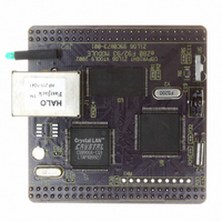
MODULE EZ80F92 512K 20MHZ
Manufacturer
Zilog
Datasheets
1.EZ80F920120MOD.pdf
(269 pages)
2.EZ80F920120MOD.pdf
(4 pages)
3.EZ80F920120MOD.pdf
(2 pages)
Specifications of EZ80F920120MOD
Module/board Type
Development Module
Processor Series
EZ80F92x
Core
eZ80
Data Bus Width
8 bit
Program Memory Type
Flash
Program Memory Size
1 MB
Interface Type
Cable
Maximum Clock Frequency
20 MHz
Operating Supply Voltage
0 V to 3.3 V
Maximum Operating Temperature
+ 70 C
Mounting Style
SMD/SMT
Package / Case
LQFP
Development Tools By Supplier
eZ80F920200ZCOG
Minimum Operating Temperature
0 C
For Use With/related Products
eZ80F92
Lead Free Status / RoHS Status
Contains lead / RoHS non-compliant
Other names
269-3157
EZ80F920120MOD
EZ80F920120MOD


Table 1. 100-Pin LQFP Pin Identification of the eZ80F92 Device (Continued)
PS015308-0404
Pin #
47
48
49
50
51
52
53
54
55
56
57
Symbol
RD
WR
INSTRD
WAIT
RESET
NMI
BUSREQ
BUSACK
HALT_SLP
V
V
DD
SS
Function
Read
Write
Instruction
Read Indicator
WAIT Request Input, Active Low
System Reset Schmitt Trigger Input,
Nonmaskable
Interrupt
Bus Request
Bus
Acknowledge
HALT and
SLEEP
Indicator
Power Supply
Ground
Signal Direction
Output, Active Low
Output, Active Low
Output, Active Low
Active Low
Schmitt Trigger Input,
Active Low
Input, Active Low
Output, Active Low
Output, Active Low
P R E L I M I N A R Y
Description
RD Low indicates that the CPU is reading
from the current address location. This pin
is tristated during bus acknowledge cycles.
WR indicates that the CPU is writing to the
current address location. This pin is
tristated during bus acknowledge cycles.
INSTRD (with MREQ and RD) indicates
the CPU is fetching an instruction from
memory. This pin is tristated during bus
acknowledge cycles.
Driving the WAIT pin Low forces the CPU
to wait additional clock cycles for an
external peripheral or external memory to
complete its Read or Write operation.
This signal is used to initialize the CPU.
This input must be Low for a minimum of 3
system clock cycles, and must be held Low
until the clock is stable. This input includes
a Schmitt trigger to allow RC rise times.
The NMI input is a higher priority input than
the maskable interrupts. It is always
recognized at the end of an instruction,
regardless of the state of the interrupt
enable control bits. This input includes a
Schmitt trigger to allow RC rise times.
External devices can request the CPU to
release the memory interface bus for their
use, by driving this pin Low.
The CPU responds to a Low on BUSREQ,
by tristating the address, data, and control
signals, and by driving the BUSACK line
Low. During bus acknowledge cycles
ADDR[23:0], IORQ, and MREQ are inputs.
A Low on this pin indicates that the CPU
has entered either HALT or SLEEP mode
because of execution of either a HALT or
SLP instruction.
Power Supply.
Ground.
Product Specification
eZ80F92/eZ80F93
Architectural Overview
11
Related parts for EZ80F920120MOD
Image
Part Number
Description
Manufacturer
Datasheet
Request
R

Part Number:
Description:
Communication Controllers, ZILOG INTELLIGENT PERIPHERAL CONTROLLER (ZIP)
Manufacturer:
Zilog, Inc.
Datasheet:

Part Number:
Description:
KIT DEV FOR Z8 ENCORE 16K TO 64K
Manufacturer:
Zilog
Datasheet:

Part Number:
Description:
KIT DEV Z8 ENCORE XP 28-PIN
Manufacturer:
Zilog
Datasheet:

Part Number:
Description:
DEV KIT FOR Z8 ENCORE 8K/4K
Manufacturer:
Zilog
Datasheet:

Part Number:
Description:
KIT DEV Z8 ENCORE XP 28-PIN
Manufacturer:
Zilog
Datasheet:

Part Number:
Description:
DEV KIT FOR Z8 ENCORE 4K TO 8K
Manufacturer:
Zilog
Datasheet:
Part Number:
Description:
CMOS Z8 microcontroller. ROM 16 Kbytes, RAM 256 bytes, speed 16 MHz, 32 lines I/O, 3.0V to 5.5V
Manufacturer:
Zilog, Inc.
Datasheet:
Part Number:
Description:
Low-cost microcontroller. 512 bytes ROM, 61 bytes RAM, 8 MHz
Manufacturer:
Zilog, Inc.
Datasheet:
Part Number:
Description:
Z8 4K OTP Microcontroller
Manufacturer:
Zilog, Inc.
Datasheet:
Part Number:
Description:
CMOS SUPER8 ROMLESS MCU
Manufacturer:
Zilog, Inc.
Datasheet:
Part Number:
Description:
SL1866 CMOSZ8 OTP Microcontroller
Manufacturer:
Zilog, Inc.
Datasheet:
Part Number:
Description:
SL1866 CMOSZ8 OTP Microcontroller
Manufacturer:
Zilog, Inc.
Datasheet:
Part Number:
Description:
OTP (KB) = 1, RAM = 125, Speed = 12, I/O = 14, 8-bit Timers = 2, Comm Interfaces Other Features = Por, LV Protect, Voltage = 4.5-5.5V
Manufacturer:
Zilog, Inc.
Datasheet:
Part Number:
Description:
Manufacturer:
Zilog, Inc.
Datasheet: