EZ80F920120MOD Zilog, EZ80F920120MOD Datasheet - Page 7
EZ80F920120MOD
Manufacturer Part Number
EZ80F920120MOD
Description
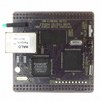
MODULE EZ80F92 512K 20MHZ
Manufacturer
Zilog
Datasheets
1.EZ80F920120MOD.pdf
(269 pages)
2.EZ80F920120MOD.pdf
(4 pages)
3.EZ80F920120MOD.pdf
(2 pages)
Specifications of EZ80F920120MOD
Module/board Type
Development Module
Processor Series
EZ80F92x
Core
eZ80
Data Bus Width
8 bit
Program Memory Type
Flash
Program Memory Size
1 MB
Interface Type
Cable
Maximum Clock Frequency
20 MHz
Operating Supply Voltage
0 V to 3.3 V
Maximum Operating Temperature
+ 70 C
Mounting Style
SMD/SMT
Package / Case
LQFP
Development Tools By Supplier
eZ80F920200ZCOG
Minimum Operating Temperature
0 C
For Use With/related Products
eZ80F92
Lead Free Status / RoHS Status
Contains lead / RoHS non-compliant
Other names
269-3157
EZ80F920120MOD
EZ80F920120MOD


List of Figures
PS015308-0404
Figure 1.
Figure 2.
Figure 3.
Figure 4.
Figure 5.
Figure 6.
Figure 7.
Figure 8.
Figure 9.
Figure 10. Example: Intel
Figure 11. Example: Intel
Figure 12. Motorola Bus Mode Signal and Pin Mapping . . . . . . . . . . . . . . . . . . . . . . . 65
Figure 13. Watch-Dog Timer Block Diagram . . . . . . . . . . . . . . . . . . . . . . . . . . . . . . . . 74
Figure 14. PRT Single Pass Mode Operation Example . . . . . . . . . . . . . . . . . . . . . . . . 80
Figure 15. UART Block Diagram . . . . . . . . . . . . . . . . . . . . . . . . . . . . . . . . . . . . . . . . 106
Figure 16. Infrared System Block Diagram . . . . . . . . . . . . . . . . . . . . . . . . . . . . . . . . 126
Figure 17. SPI Master Device . . . . . . . . . . . . . . . . . . . . . . . . . . . . . . . . . . . . . . . . . . . 132
Figure 18. SPI Slave Device . . . . . . . . . . . . . . . . . . . . . . . . . . . . . . . . . . . . . . . . . . . . 132
Figure 19. I
Figure 20. START and STOP Conditions In I
Figure 21. I
Figure 22. Clock Synchronization In I
Figure 23. Typical ZDI Debug Setup . . . . . . . . . . . . . . . . . . . . . . . . . . . . . . . . . . . . . 163
Figure 24. Schematic For Building a Target Board ZPAK II Connector . . . . . . . . . . 164
Figure 25. ZDI Write Timing . . . . . . . . . . . . . . . . . . . . . . . . . . . . . . . . . . . . . . . . . . . 165
Figure 26. ZDI Read Timing . . . . . . . . . . . . . . . . . . . . . . . . . . . . . . . . . . . . . . . . . . . . 166
Figure 27. ZDI Address Write Timing . . . . . . . . . . . . . . . . . . . . . . . . . . . . . . . . . . . . 167
Figure 28. eZ80F92 On-Chip RAM Memory Addressing Example . . . . . . . . . . . . . . 193
Figure 29. eZ80F93 On-Chip RAM Memory Addressing Example . . . . . . . . . . . . . . 194
Figure 30. Recommended Crystal Oscillator Configuration (20MHz operation) . . . . 223
Figure 31. Recommended Crystal Oscillator Configuration (32KHz operation) . . . . 224
Figure 32. ICC Versus WAIT States as a Function of Frequency . . . . . . . . . . . . . . . 229
Figure 33. ICC Versus Frequency as a Function of WAIT States . . . . . . . . . . . . . . . 230
Figure 34. ICC Versus Temperature as a Function of Frequency . . . . . . . . . . . . . . . . 231
eZ80F92 Block Diagram . . . . . . . . . . . . . . . . . . . . . . . . . . . . . . . . . . . . . . . . 3
100-Pin LQFP Configuration of the eZ80F92 Device . . . . . . . . . . . . . . . . . . 4
GPIO Port Pin Block Diagram . . . . . . . . . . . . . . . . . . . . . . . . . . . . . . . . . . . 44
Example: Memory Chip Select . . . . . . . . . . . . . . . . . . . . . . . . . . . . . . . . . . 51
Wait Input Sampling Block Diagram . . . . . . . . . . . . . . . . . . . . . . . . . . . . . 53
Example: Z80 Bus Mode Write Timing . . . . . . . . . . . . . . . . . . . . . . . . . . . 57
Intel Bus Mode Signal and Pin Mapping . . . . . . . . . . . . . . . . . . . . . . . . . . . 58
Example: Intel Bus Mode Read Timing—Separate Address
and Data Buses . . . . . . . . . . . . . . . . . . . . . . . . . . . . . . . . . . . . . . . . . . . . . . . 60
Example: Intel Bus Mode Write Timing—Separate Address
and Data Buses . . . . . . . . . . . . . . . . . . . . . . . . . . . . . . . . . . . . . . . . . . . . . . . 61
and Data Bus . . . . . . . . . . . . . . . . . . . . . . . . . . . . . . . . . . . . . . . . . . . . . . . . 63
and Data Bus . . . . . . . . . . . . . . . . . . . . . . . . . . . . . . . . . . . . . . . . . . . . . . . . 64
2
2
C Clock and Data Relationship . . . . . . . . . . . . . . . . . . . . . . . . . . . . . . . . 143
C Acknowledge . . . . . . . . . . . . . . . . . . . . . . . . . . . . . . . . . . . . . . . . . . . . 145
TM
TM
P R E L I M I N A R Y
Bus Mode Read Timing—Multiplexed Address
Bus Mode Write Timing—Multiplexed Address
2
C Protocol . . . . . . . . . . . . . . . . . . . . . . . . . . . 146
2
C Protocol . . . . . . . . . . . . . . . . . . . . . 143
Product Specification
eZ80F92/eZ80F93
List of Figures
vii
Related parts for EZ80F920120MOD
Image
Part Number
Description
Manufacturer
Datasheet
Request
R

Part Number:
Description:
Communication Controllers, ZILOG INTELLIGENT PERIPHERAL CONTROLLER (ZIP)
Manufacturer:
Zilog, Inc.
Datasheet:

Part Number:
Description:
KIT DEV FOR Z8 ENCORE 16K TO 64K
Manufacturer:
Zilog
Datasheet:

Part Number:
Description:
KIT DEV Z8 ENCORE XP 28-PIN
Manufacturer:
Zilog
Datasheet:

Part Number:
Description:
DEV KIT FOR Z8 ENCORE 8K/4K
Manufacturer:
Zilog
Datasheet:

Part Number:
Description:
KIT DEV Z8 ENCORE XP 28-PIN
Manufacturer:
Zilog
Datasheet:

Part Number:
Description:
DEV KIT FOR Z8 ENCORE 4K TO 8K
Manufacturer:
Zilog
Datasheet:
Part Number:
Description:
CMOS Z8 microcontroller. ROM 16 Kbytes, RAM 256 bytes, speed 16 MHz, 32 lines I/O, 3.0V to 5.5V
Manufacturer:
Zilog, Inc.
Datasheet:
Part Number:
Description:
Low-cost microcontroller. 512 bytes ROM, 61 bytes RAM, 8 MHz
Manufacturer:
Zilog, Inc.
Datasheet:
Part Number:
Description:
Z8 4K OTP Microcontroller
Manufacturer:
Zilog, Inc.
Datasheet:
Part Number:
Description:
CMOS SUPER8 ROMLESS MCU
Manufacturer:
Zilog, Inc.
Datasheet:
Part Number:
Description:
SL1866 CMOSZ8 OTP Microcontroller
Manufacturer:
Zilog, Inc.
Datasheet:
Part Number:
Description:
SL1866 CMOSZ8 OTP Microcontroller
Manufacturer:
Zilog, Inc.
Datasheet:
Part Number:
Description:
OTP (KB) = 1, RAM = 125, Speed = 12, I/O = 14, 8-bit Timers = 2, Comm Interfaces Other Features = Por, LV Protect, Voltage = 4.5-5.5V
Manufacturer:
Zilog, Inc.
Datasheet:
Part Number:
Description:
Manufacturer:
Zilog, Inc.
Datasheet: