EZ80F920120MOD Zilog, EZ80F920120MOD Datasheet - Page 74
EZ80F920120MOD
Manufacturer Part Number
EZ80F920120MOD
Description
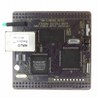
MODULE EZ80F92 512K 20MHZ
Manufacturer
Zilog
Datasheets
1.EZ80F920120MOD.pdf
(269 pages)
2.EZ80F920120MOD.pdf
(4 pages)
3.EZ80F920120MOD.pdf
(2 pages)
Specifications of EZ80F920120MOD
Module/board Type
Development Module
Processor Series
EZ80F92x
Core
eZ80
Data Bus Width
8 bit
Program Memory Type
Flash
Program Memory Size
1 MB
Interface Type
Cable
Maximum Clock Frequency
20 MHz
Operating Supply Voltage
0 V to 3.3 V
Maximum Operating Temperature
+ 70 C
Mounting Style
SMD/SMT
Package / Case
LQFP
Development Tools By Supplier
eZ80F920200ZCOG
Minimum Operating Temperature
0 C
For Use With/related Products
eZ80F92
Lead Free Status / RoHS Status
Contains lead / RoHS non-compliant
Other names
269-3157
EZ80F920120MOD
EZ80F920120MOD


PS015308-0404
Intel Bus Mode (Multiplexed Address and Data Bus)
During Read operations with multiplexed address and data, the Intel
4 states (T1, T2, T3, and T4) as described in Intel Bus Mode Read States (Multiplexed
Address and Data Bus).
Table 18. Intel Bus Mode Read States (Multiplexed Address and Data Bus)
During Write operations with multiplexed address and data, the Intel
employs 4 states (T1, T2, T3, and T4) as described in Intel Bus Mode Write States (Multi-
plexed Address and Data Bus).
Table 19. Intel Bus Mode Write States (Multiplexed Address and Data Bus)
STATE T1
STATE T2
STATE T3
STATE T4
STATE T1
STATE T2
STATE T3
STATE T4
The Read cycle begins in State T1. The CPU drives the address onto the
DATA bus and the associated Chip Select signal is asserted. The CPU
drives the ALE signal High at the beginning of T1. During the middle of T1,
the CPU drives ALE Low to facilitate the latching of the address.
During State T2, the CPU removes the address from the DATA bus and
asserts the RD signal. Depending upon the instruction, either the MREQ
or IORQ signal is asserted.
During State T3, no bus signals are altered. If the external READY (WAIT)
pin is driven Low at least one CPU system clock cycle prior to the
beginning of State T3, additional WAIT states (T
the READY pin is driven High.
The CPU latches the Read data at the beginning of State T4. The CPU
deasserts the RD signal and completes the Intel
The Write cycle begins in State T1. The CPU drives the address onto the
DATA bus and drives the ALE signal High at the beginning of T1. During
the middle of T1, the CPU drives ALE Low to facilitate the latching of the
address.
During State T2, the CPU removes the address from the DATA bus and
drives the Write data onto the DATA bus. The WR signal is asserted to
indicate a Write operation.
During State T3, no bus signals are altered. If the external READY (WAIT)
pin is driven Low at least one CPU system clock cycle prior to the
beginning of State T3, additional wait states (T
READY pin is driven High.
The CPU deasserts the Write signal at the beginning of T4 identifying the
end of the Write operation. The CPU holds the data and address buses
through the end of T4. The bus cycle is completed at the end of T4.
P R E L I M I N A R Y
WAIT
WAIT
TM
Chip Selects and Wait States
Product Specification
) are asserted until the
bus mode cycle.
TM
) are asserted until
TM
eZ80F92/eZ80F93
bus mode employs
bus mode
62
Related parts for EZ80F920120MOD
Image
Part Number
Description
Manufacturer
Datasheet
Request
R

Part Number:
Description:
Communication Controllers, ZILOG INTELLIGENT PERIPHERAL CONTROLLER (ZIP)
Manufacturer:
Zilog, Inc.
Datasheet:

Part Number:
Description:
KIT DEV FOR Z8 ENCORE 16K TO 64K
Manufacturer:
Zilog
Datasheet:

Part Number:
Description:
KIT DEV Z8 ENCORE XP 28-PIN
Manufacturer:
Zilog
Datasheet:

Part Number:
Description:
DEV KIT FOR Z8 ENCORE 8K/4K
Manufacturer:
Zilog
Datasheet:

Part Number:
Description:
KIT DEV Z8 ENCORE XP 28-PIN
Manufacturer:
Zilog
Datasheet:

Part Number:
Description:
DEV KIT FOR Z8 ENCORE 4K TO 8K
Manufacturer:
Zilog
Datasheet:
Part Number:
Description:
CMOS Z8 microcontroller. ROM 16 Kbytes, RAM 256 bytes, speed 16 MHz, 32 lines I/O, 3.0V to 5.5V
Manufacturer:
Zilog, Inc.
Datasheet:
Part Number:
Description:
Low-cost microcontroller. 512 bytes ROM, 61 bytes RAM, 8 MHz
Manufacturer:
Zilog, Inc.
Datasheet:
Part Number:
Description:
Z8 4K OTP Microcontroller
Manufacturer:
Zilog, Inc.
Datasheet:
Part Number:
Description:
CMOS SUPER8 ROMLESS MCU
Manufacturer:
Zilog, Inc.
Datasheet:
Part Number:
Description:
SL1866 CMOSZ8 OTP Microcontroller
Manufacturer:
Zilog, Inc.
Datasheet:
Part Number:
Description:
SL1866 CMOSZ8 OTP Microcontroller
Manufacturer:
Zilog, Inc.
Datasheet:
Part Number:
Description:
OTP (KB) = 1, RAM = 125, Speed = 12, I/O = 14, 8-bit Timers = 2, Comm Interfaces Other Features = Por, LV Protect, Voltage = 4.5-5.5V
Manufacturer:
Zilog, Inc.
Datasheet:
Part Number:
Description:
Manufacturer:
Zilog, Inc.
Datasheet: