EZ80F920120MOD Zilog, EZ80F920120MOD Datasheet - Page 211
EZ80F920120MOD
Manufacturer Part Number
EZ80F920120MOD
Description
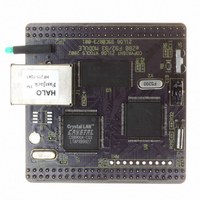
MODULE EZ80F92 512K 20MHZ
Manufacturer
Zilog
Datasheets
1.EZ80F920120MOD.pdf
(269 pages)
2.EZ80F920120MOD.pdf
(4 pages)
3.EZ80F920120MOD.pdf
(2 pages)
Specifications of EZ80F920120MOD
Module/board Type
Development Module
Processor Series
EZ80F92x
Core
eZ80
Data Bus Width
8 bit
Program Memory Type
Flash
Program Memory Size
1 MB
Interface Type
Cable
Maximum Clock Frequency
20 MHz
Operating Supply Voltage
0 V to 3.3 V
Maximum Operating Temperature
+ 70 C
Mounting Style
SMD/SMT
Package / Case
LQFP
Development Tools By Supplier
eZ80F920200ZCOG
Minimum Operating Temperature
0 C
For Use With/related Products
eZ80F92
Lead Free Status / RoHS Status
Contains lead / RoHS non-compliant
Other names
269-3157
EZ80F920120MOD
EZ80F920120MOD


PS015308-0404
A typical sequence that performs a single-byte I/O Write is detailed below. Because the
Write is self-timed, the sequence can be repeated back-to-back without any necessity for
polling or interrupts.
1. Write the FLASH_PAGE, FLASH_ROW, and FLASH_COL registers with the
2. Write the data value to the FLASH_DATA register.
Multibyte I/O Write (Row Programming)
Multibyte I/O Write operations use the same I/O registers as single-byte Writes, but use an
internal address incrementer for subsequent Writes. Multibyte Writes allow programming
of a full row and are enabled by setting the ROW_PGM bit of the Flash Program Control
Register. For multibyte Writes, the CPU sets the address registers, enables row program-
ming, and then executes a output to I/O instruction with repeat to load the block of data
into the FLASH_DATA register. For each individual byte written to the FLASH_DATA
register during the block move, the Flash controller asserts the internal WAIT signal to
stall the CPU until the current byte has been programmed.
During row programming, the Flash controller continuously asserts Flash’s high voltage
until all bytes are programmed (column address < 127). As a consequence, the row can be
programmed faster than if the high voltage is toggled for each byte. The per-byte program-
ming time during row programming is between 41 µs and 52 µs. As such, programming the
128 bytes of a row in this mode takes at most 6.7 ms, leaving 9.3 ms for the overhead of
CPU instructions used to fetch the 128 bytes.
A typical sequence that performs a multibyte I/O Write is shown in the following
sequence.
1. Check the FLASH_IRQ register to be sure any previous Row Program has completed.
2. Write the FLASH_PAGE, FLASH_ROW, and FLASH_COL registers with the
3. Set the ROW_PGM bit in the FLASH_PGCTL register to enable row programming
4. Write the next data value to the FLASH_DATA register.
5. If the end of the row has not been reached, return to Step 4.
During row programming, software must monitor the row time-out error bit either by
enabling this interrupt or through polling. If a row time-out occurs, the Flash controller
aborts the row programming operation and software must then assure that no further
writes are performed to the row without it first being erased. It is suggested that row pro-
gramming only be used one time per row and not in combination with single-byte Writes
to the same row without first erasing it. Otherwise, the burden is on software to ensure that
address of the byte to be written.
address of the first byte to be written.
mode.
P R E L I M I N A R Y
Product Specification
eZ80F92/eZ80F93
Flash Memory
199
Related parts for EZ80F920120MOD
Image
Part Number
Description
Manufacturer
Datasheet
Request
R

Part Number:
Description:
Communication Controllers, ZILOG INTELLIGENT PERIPHERAL CONTROLLER (ZIP)
Manufacturer:
Zilog, Inc.
Datasheet:

Part Number:
Description:
KIT DEV FOR Z8 ENCORE 16K TO 64K
Manufacturer:
Zilog
Datasheet:

Part Number:
Description:
KIT DEV Z8 ENCORE XP 28-PIN
Manufacturer:
Zilog
Datasheet:

Part Number:
Description:
DEV KIT FOR Z8 ENCORE 8K/4K
Manufacturer:
Zilog
Datasheet:

Part Number:
Description:
KIT DEV Z8 ENCORE XP 28-PIN
Manufacturer:
Zilog
Datasheet:

Part Number:
Description:
DEV KIT FOR Z8 ENCORE 4K TO 8K
Manufacturer:
Zilog
Datasheet:
Part Number:
Description:
CMOS Z8 microcontroller. ROM 16 Kbytes, RAM 256 bytes, speed 16 MHz, 32 lines I/O, 3.0V to 5.5V
Manufacturer:
Zilog, Inc.
Datasheet:
Part Number:
Description:
Low-cost microcontroller. 512 bytes ROM, 61 bytes RAM, 8 MHz
Manufacturer:
Zilog, Inc.
Datasheet:
Part Number:
Description:
Z8 4K OTP Microcontroller
Manufacturer:
Zilog, Inc.
Datasheet:
Part Number:
Description:
CMOS SUPER8 ROMLESS MCU
Manufacturer:
Zilog, Inc.
Datasheet:
Part Number:
Description:
SL1866 CMOSZ8 OTP Microcontroller
Manufacturer:
Zilog, Inc.
Datasheet:
Part Number:
Description:
SL1866 CMOSZ8 OTP Microcontroller
Manufacturer:
Zilog, Inc.
Datasheet:
Part Number:
Description:
OTP (KB) = 1, RAM = 125, Speed = 12, I/O = 14, 8-bit Timers = 2, Comm Interfaces Other Features = Por, LV Protect, Voltage = 4.5-5.5V
Manufacturer:
Zilog, Inc.
Datasheet:
Part Number:
Description:
Manufacturer:
Zilog, Inc.
Datasheet: