EZ80F920120MOD Zilog, EZ80F920120MOD Datasheet - Page 261
EZ80F920120MOD
Manufacturer Part Number
EZ80F920120MOD
Description
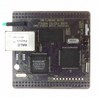
MODULE EZ80F92 512K 20MHZ
Manufacturer
Zilog
Datasheets
1.EZ80F920120MOD.pdf
(269 pages)
2.EZ80F920120MOD.pdf
(4 pages)
3.EZ80F920120MOD.pdf
(2 pages)
Specifications of EZ80F920120MOD
Module/board Type
Development Module
Processor Series
EZ80F92x
Core
eZ80
Data Bus Width
8 bit
Program Memory Type
Flash
Program Memory Size
1 MB
Interface Type
Cable
Maximum Clock Frequency
20 MHz
Operating Supply Voltage
0 V to 3.3 V
Maximum Operating Temperature
+ 70 C
Mounting Style
SMD/SMT
Package / Case
LQFP
Development Tools By Supplier
eZ80F920200ZCOG
Minimum Operating Temperature
0 C
For Use With/related Products
eZ80F92
Lead Free Status / RoHS Status
Contains lead / RoHS non-compliant
Other names
269-3157
EZ80F920120MOD
EZ80F920120MOD


CPHA—see Clock Phase
CPOL—see Clock Polarity
CPU system clock cycle 56
CS0 9, 21, 50–53
CS1 9, 21, 50–53
CS2 9, 21, 50, 52–53
CS3 9, 21, 50, 52–53
CTS—see Clear To Send
CTS0 14, 130
CTS1 16
Customer Feedback Form 258
cycle termination signal 66
D
data bus 9, 54, 55, 57–59, 62, 66, 72, 92, 170, 181,
Data Carrier Detect 14, 17, 121, 124
Data Set Ready 14, 16, 122, 124
Data Terminal Ready 14, 16, 122, 124
Data Transfer Procedure with SPI configured as a
Data Transfer Procedure with SPI Configured as
data transfer, SPI 140
Data Validity 143
DC Characteristics 226
DCD—see Data Carrier Detect
DCD0 14, 130
DCD1 17
DCTS—see Clear To Send, Delta Status Change of
DDCD —see Data Carrier Detect, Delta Status
DDSR —see Data Set Ready, Delta Status Change
divisor count 112, 137
Document Information 247
Document Number Description 247
DSR—see Data Set Ready
DSR0 14, 130
DSR1 16
DTACK—see cycle termination signal
PS015308-0404
187
Slave 137
the Master 136
Change of
of
Delta Status Change of 125
Delta Status Change of 125
P R E L I M I N A R Y
DTR—see Data Terminal Ready
DTR0 14, 130
DTR1 16
E
edge-selectable interrupts 45
edge-triggered interrupt input 130
edge-triggered interrupt mode 43, 45
Edge-Triggered Interrupts 44
EI, Op Code Map 216
Electrical Characteristics 226
ENAB—see Bus Enable bit
Enabling and Disabling the WDT 75
endec—see Infrared Encoder/Decoder
Erase operations 196–197
Event Counter 82
External Bus Acknowledge Timing 242
external bus request 54, 166, 170
External I/O Chip Selects 25
External I/O Read Timing 237
External I/O Write Timing 238
External Memory Read Timing 234
External Memory Write Timing 235
external pull-down resistor 42
External System Clock Driver (PHI) Timing 242
eZ80 Bus mode 55, 68, 72
eZ80 CPU 10, 37, 54, 58, 59, 66, 172, 190
eZ80 Product ID Low and High Byte Registers 184
eZ80 Product ID Revision Register 185
eZ80
eZ80F92 device 1–4, 5, 9, 25, 37, 41, 47–48, 50, 52,
F
FAST mode 142, 162
Features, eZ80 CPU Core 33
Flash memory 1, 194, 196
68, 74, 78, 82, 110, 111, 154, 164–166, 168, 172,
177–178, 182–183, 185, 187, 223, 226, 228, 233,
242
Core 33
Instruction Set 211
Arrangement in the eZ80F93 197
®
system clock cycle 55–56, 59, 62
Product Specification
eZ80F92/eZ80F93
Index
249
Related parts for EZ80F920120MOD
Image
Part Number
Description
Manufacturer
Datasheet
Request
R

Part Number:
Description:
Communication Controllers, ZILOG INTELLIGENT PERIPHERAL CONTROLLER (ZIP)
Manufacturer:
Zilog, Inc.
Datasheet:

Part Number:
Description:
KIT DEV FOR Z8 ENCORE 16K TO 64K
Manufacturer:
Zilog
Datasheet:

Part Number:
Description:
KIT DEV Z8 ENCORE XP 28-PIN
Manufacturer:
Zilog
Datasheet:

Part Number:
Description:
DEV KIT FOR Z8 ENCORE 8K/4K
Manufacturer:
Zilog
Datasheet:

Part Number:
Description:
KIT DEV Z8 ENCORE XP 28-PIN
Manufacturer:
Zilog
Datasheet:

Part Number:
Description:
DEV KIT FOR Z8 ENCORE 4K TO 8K
Manufacturer:
Zilog
Datasheet:
Part Number:
Description:
CMOS Z8 microcontroller. ROM 16 Kbytes, RAM 256 bytes, speed 16 MHz, 32 lines I/O, 3.0V to 5.5V
Manufacturer:
Zilog, Inc.
Datasheet:
Part Number:
Description:
Low-cost microcontroller. 512 bytes ROM, 61 bytes RAM, 8 MHz
Manufacturer:
Zilog, Inc.
Datasheet:
Part Number:
Description:
Z8 4K OTP Microcontroller
Manufacturer:
Zilog, Inc.
Datasheet:
Part Number:
Description:
CMOS SUPER8 ROMLESS MCU
Manufacturer:
Zilog, Inc.
Datasheet:
Part Number:
Description:
SL1866 CMOSZ8 OTP Microcontroller
Manufacturer:
Zilog, Inc.
Datasheet:
Part Number:
Description:
SL1866 CMOSZ8 OTP Microcontroller
Manufacturer:
Zilog, Inc.
Datasheet:
Part Number:
Description:
OTP (KB) = 1, RAM = 125, Speed = 12, I/O = 14, 8-bit Timers = 2, Comm Interfaces Other Features = Por, LV Protect, Voltage = 4.5-5.5V
Manufacturer:
Zilog, Inc.
Datasheet:
Part Number:
Description:
Manufacturer:
Zilog, Inc.
Datasheet: