EZ80F920120MOD Zilog, EZ80F920120MOD Datasheet - Page 37
EZ80F920120MOD
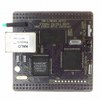
Manufacturer Part Number
EZ80F920120MOD
Description
MODULE EZ80F92 512K 20MHZ
Manufacturer
Zilog
Datasheets
1.EZ80F920120MOD.pdf
(269 pages)
2.EZ80F920120MOD.pdf
(4 pages)
3.EZ80F920120MOD.pdf
(2 pages)
Specifications of EZ80F920120MOD
Module/board Type
Development Module
Processor Series
EZ80F92x
Core
eZ80
Data Bus Width
8 bit
Program Memory Type
Flash
Program Memory Size
1 MB
Interface Type
Cable
Maximum Clock Frequency
20 MHz
Operating Supply Voltage
0 V to 3.3 V
Maximum Operating Temperature
+ 70 C
Mounting Style
SMD/SMT
Package / Case
LQFP
Development Tools By Supplier
eZ80F920200ZCOG
Minimum Operating Temperature
0 C
For Use With/related Products
eZ80F92
Lead Free Status / RoHS Status
Contains lead / RoHS non-compliant
Other names
269-3157
EZ80F920120MOD
EZ80F920120MOD


Register Map
Table 3. Register Map
PS015308-0404
Address
(hex)
Programmable Reload Counter/Timers
0080
0081
0082
0083
0084
0085
0086
Notes:
1. After an external pin reset, the Watch-Dog Timer Control register is reset to 00h. After a Watch-Dog Timer time-
2. When the CPU reads this register, the current sampled value of the port is read.
3. Read Only if RTC registers are locked; Read/Write if RTC registers are unlocked.
4. After an external pin reset or a Watch-Dog Timer reset, the RTC Control register is reset to x0xxxx00b. After an
5. Read Only if Flash Memory is locked. Read/Write if Flash Memory is unlocked.
out reset, the Watch-Dog Timer Control register is reset to 20h.
RTC Alarm sleep-mode recovery reset, the RTC Control register is reset to x0xxxx10b.
Mnemonic
TMR0_CTL
TMR0_DR_L
TMR0_RR_L
TMR0_DR_H
TMR0_RR_H
TMR1_CTL
TMR1_DR_L
TMR1_RR_L
TMR1_DR_H
TMR1_RR_H
TMR2_CTL
All on-chip peripheral registers are accessed in the I/O address space. All I/O operations
employ 16-bit addresses. The upper byte of the 24-bit address bus is undefined during all
I/O operations (ADDR[23:16] =
range
not generated if the address space programmed for the I/O Chip Selects overlaps the
0080h–00FFh
Registers at unused addresses within the
erals are not implemented. Read access to such addresses returns unpredictable values and
Write access produces no effect. Register Map diagrams the register map for the eZ80F92
device.
0080h–00FFh
Name
Timer 0 Control Register
Timer 0 Data Register—Low Byte
Timer 0 Reload Register—Low Byte
Timer 0 Data Register—High Byte
Timer 0 Reload Register—High Byte
Timer 1 Control Register
Timer 1 Data Register—Low Byte
Timer 1 Reload Register—Low Byte
Timer 1 Data Register—High Byte
Timer 1 Reload Register—High Byte
Timer 2 Control Register
address range.
are routed to the on-chip peripherals. External I/O Chip Selects are
P R E L I M I N A R Y
UU
). All I/O operations using 16-bit addresses within the
0080h–00FFh
range assigned to on-chip periph-
Reset
(hex)
00
00
00
00
00
00
00
00
00
00
00
Product Specification
eZ80F92/eZ80F93
Access
CPU
R/W
R/W
R/W
W
W
W
W
R
R
R
R
Register Map
Page
85
86
87
87
88
85
86
87
87
88
85
#
25
Related parts for EZ80F920120MOD
Image
Part Number
Description
Manufacturer
Datasheet
Request
R

Part Number:
Description:
Communication Controllers, ZILOG INTELLIGENT PERIPHERAL CONTROLLER (ZIP)
Manufacturer:
Zilog, Inc.
Datasheet:

Part Number:
Description:
KIT DEV FOR Z8 ENCORE 16K TO 64K
Manufacturer:
Zilog
Datasheet:

Part Number:
Description:
KIT DEV Z8 ENCORE XP 28-PIN
Manufacturer:
Zilog
Datasheet:

Part Number:
Description:
DEV KIT FOR Z8 ENCORE 8K/4K
Manufacturer:
Zilog
Datasheet:

Part Number:
Description:
KIT DEV Z8 ENCORE XP 28-PIN
Manufacturer:
Zilog
Datasheet:

Part Number:
Description:
DEV KIT FOR Z8 ENCORE 4K TO 8K
Manufacturer:
Zilog
Datasheet:
Part Number:
Description:
CMOS Z8 microcontroller. ROM 16 Kbytes, RAM 256 bytes, speed 16 MHz, 32 lines I/O, 3.0V to 5.5V
Manufacturer:
Zilog, Inc.
Datasheet:
Part Number:
Description:
Low-cost microcontroller. 512 bytes ROM, 61 bytes RAM, 8 MHz
Manufacturer:
Zilog, Inc.
Datasheet:
Part Number:
Description:
Z8 4K OTP Microcontroller
Manufacturer:
Zilog, Inc.
Datasheet:
Part Number:
Description:
CMOS SUPER8 ROMLESS MCU
Manufacturer:
Zilog, Inc.
Datasheet:
Part Number:
Description:
SL1866 CMOSZ8 OTP Microcontroller
Manufacturer:
Zilog, Inc.
Datasheet:
Part Number:
Description:
SL1866 CMOSZ8 OTP Microcontroller
Manufacturer:
Zilog, Inc.
Datasheet:
Part Number:
Description:
OTP (KB) = 1, RAM = 125, Speed = 12, I/O = 14, 8-bit Timers = 2, Comm Interfaces Other Features = Por, LV Protect, Voltage = 4.5-5.5V
Manufacturer:
Zilog, Inc.
Datasheet:
Part Number:
Description:
Manufacturer:
Zilog, Inc.
Datasheet: