EZ80F920120MOD Zilog, EZ80F920120MOD Datasheet - Page 210
EZ80F920120MOD
Manufacturer Part Number
EZ80F920120MOD
Description
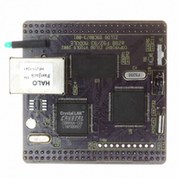
MODULE EZ80F92 512K 20MHZ
Manufacturer
Zilog
Datasheets
1.EZ80F920120MOD.pdf
(269 pages)
2.EZ80F920120MOD.pdf
(4 pages)
3.EZ80F920120MOD.pdf
(2 pages)
Specifications of EZ80F920120MOD
Module/board Type
Development Module
Processor Series
EZ80F92x
Core
eZ80
Data Bus Width
8 bit
Program Memory Type
Flash
Program Memory Size
1 MB
Interface Type
Cable
Maximum Clock Frequency
20 MHz
Operating Supply Voltage
0 V to 3.3 V
Maximum Operating Temperature
+ 70 C
Mounting Style
SMD/SMT
Package / Case
LQFP
Development Tools By Supplier
eZ80F920200ZCOG
Minimum Operating Temperature
0 C
For Use With/related Products
eZ80F92
Lead Free Status / RoHS Status
Contains lead / RoHS non-compliant
Other names
269-3157
EZ80F920120MOD
EZ80F920120MOD


Figure 49.Flash Memory Block Diagram
PS015308-0404
eZ80 Core
Programming Flash Memory
Interface
System Clock
Caution:
Flash memory is programmed using standard I/O or memory Write operations which the
Flash memory controller automatically translates to the detailed timing and protocol
required for Flash memory. The more efficient multibyte (row) programming mode is only
available via I/O Writes.
1. The cumulative programming time subsequent to the most recent Erase cannot exceed
2. The same byte cannot be programmed more than twice subsequent to the most recent
Single-Byte I/O Write Operations
A single-byte I/O Write operation uses I/O registers for setting the column, page, and row
address to be programmed. The FLASH_DATA register stores the data to be written.
While the CPU executes an output to I/O instruction to load the data into the
FLASH_DATA register, the Flash controller asserts the internal WAIT signal to stall the
CPU until the Flash Write operation is complete. A single-byte Write takes between 66 µs
and 85µs to complete. Programming an entire row (128 bytes) using single-byte Writes
therefore takes at most 10.8 ms. This measure of time does not include the time required
by the CPU to transfer data to the registers, which is a function of the instructions
employed and the system clock frequency.
ADDR
D
16 ms for any given row.
Erase.
OUT
17
To ensure data integrity and device reliability, two main restrictions exist when
programming Flash memory:
8
Registers
8-bit downcounter
Control
Flash
Clock Divider
P R E L I M I N A R Y
Machine
Flash
State
FADDR
FD
FCNTL
MAIN_INFO
CPUD
FLASH_IRQ
IN
OUT
17
8
9
8
Product Specification
512 bytes
256 KB
Flash
+
eZ80F92/eZ80F93
FD
Flash Memory
OUT
8
198
Related parts for EZ80F920120MOD
Image
Part Number
Description
Manufacturer
Datasheet
Request
R

Part Number:
Description:
Communication Controllers, ZILOG INTELLIGENT PERIPHERAL CONTROLLER (ZIP)
Manufacturer:
Zilog, Inc.
Datasheet:

Part Number:
Description:
KIT DEV FOR Z8 ENCORE 16K TO 64K
Manufacturer:
Zilog
Datasheet:

Part Number:
Description:
KIT DEV Z8 ENCORE XP 28-PIN
Manufacturer:
Zilog
Datasheet:

Part Number:
Description:
DEV KIT FOR Z8 ENCORE 8K/4K
Manufacturer:
Zilog
Datasheet:

Part Number:
Description:
KIT DEV Z8 ENCORE XP 28-PIN
Manufacturer:
Zilog
Datasheet:

Part Number:
Description:
DEV KIT FOR Z8 ENCORE 4K TO 8K
Manufacturer:
Zilog
Datasheet:
Part Number:
Description:
CMOS Z8 microcontroller. ROM 16 Kbytes, RAM 256 bytes, speed 16 MHz, 32 lines I/O, 3.0V to 5.5V
Manufacturer:
Zilog, Inc.
Datasheet:
Part Number:
Description:
Low-cost microcontroller. 512 bytes ROM, 61 bytes RAM, 8 MHz
Manufacturer:
Zilog, Inc.
Datasheet:
Part Number:
Description:
Z8 4K OTP Microcontroller
Manufacturer:
Zilog, Inc.
Datasheet:
Part Number:
Description:
CMOS SUPER8 ROMLESS MCU
Manufacturer:
Zilog, Inc.
Datasheet:
Part Number:
Description:
SL1866 CMOSZ8 OTP Microcontroller
Manufacturer:
Zilog, Inc.
Datasheet:
Part Number:
Description:
SL1866 CMOSZ8 OTP Microcontroller
Manufacturer:
Zilog, Inc.
Datasheet:
Part Number:
Description:
OTP (KB) = 1, RAM = 125, Speed = 12, I/O = 14, 8-bit Timers = 2, Comm Interfaces Other Features = Por, LV Protect, Voltage = 4.5-5.5V
Manufacturer:
Zilog, Inc.
Datasheet:
Part Number:
Description:
Manufacturer:
Zilog, Inc.
Datasheet: