EZ80F920120MOD Zilog, EZ80F920120MOD Datasheet - Page 147
EZ80F920120MOD
Manufacturer Part Number
EZ80F920120MOD
Description
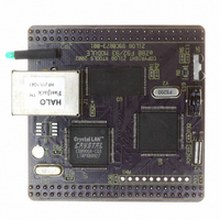
MODULE EZ80F92 512K 20MHZ
Manufacturer
Zilog
Datasheets
1.EZ80F920120MOD.pdf
(269 pages)
2.EZ80F920120MOD.pdf
(4 pages)
3.EZ80F920120MOD.pdf
(2 pages)
Specifications of EZ80F920120MOD
Module/board Type
Development Module
Processor Series
EZ80F92x
Core
eZ80
Data Bus Width
8 bit
Program Memory Type
Flash
Program Memory Size
1 MB
Interface Type
Cable
Maximum Clock Frequency
20 MHz
Operating Supply Voltage
0 V to 3.3 V
Maximum Operating Temperature
+ 70 C
Mounting Style
SMD/SMT
Package / Case
LQFP
Development Tools By Supplier
eZ80F920200ZCOG
Minimum Operating Temperature
0 C
For Use With/related Products
eZ80F92
Lead Free Status / RoHS Status
Contains lead / RoHS non-compliant
Other names
269-3157
EZ80F920120MOD
EZ80F920120MOD


PS015308-0404
SPI Functional Description
SPI Flags
When a master transmits to a slave device via the MOSI signal, the slave device responds
by sending data to the master via the master's MISO signal. The resulting implication is a
full-duplex transmission, with both data out and data in synchronized with the same clock
signal. Thus the byte transmitted is replaced by the byte received and eliminates the
requirement for separate transmit-empty and receive-full status bits. A single status bit,
SPIF, is used to signify that the I/O operation is completed, see the SPI Status Register
(SPI_SR) on page 140.
The SPI is double-buffered on Read, but not on Write. If a Write is performed during data
transfer, the transfer occurs uninterrupted, and the Write is unsuccessful. This condition
causes the WRITE COLLISION (WCOL) status bit in the SPI_SR register to be set. After
a data byte is shifted, the SPIF flag of the SPI_SR register is set.
In SPI MASTER mode, the SCK pin functions as an output. It idles High or Low, depend-
ing on the CPOL bit in the SPI_CTL register, until data is written to the shift register. Data
transfer is initiated by writing to the transmit shift register, SPI_TSR. Eight clocks are then
generated to shift the eight bits of transmit data out the MOSI pin while shifting in eight
bits of data on the MISO pin. After transfer, the SCK signal idles.
In SPI SLAVE mode, the start logic receives a logic Low from the SS pin and a clock input
at the SCK pin, and the slave is synchronized to the master. Data from the master is
received serially from the slave MOSI signal and loads the 8-bit shift register. After the 8-
bit shift register is loaded, its data is parallel transferred to the Read buffer. During a Write
cycle data is written into the shift register, then the slave waits for the SPI master to initiate
a data transfer, supply a clock signal, and shift the data out on the slave's MISO signal.
If the CPHA bit in the SPI_CTL register is 0, a transfer begins when SS pin signal goes
Low and the transfer ends when SS goes High after eight clock cycles on SCK. When the
CPHA bit is set to 1, a transfer begins the first time SCK becomes active while SS is Low
and the transfer ends when the SPIF flag gets set.
Mode Fault
The Mode Fault flag (MODF) indicates that there may be a multimaster conflict for sys-
tem control. The MODF bit is normally cleared to 0 and is only set to 1 when the master
device’s SS pin is pulled Low. When a mode fault is detected, the following occurs:
1. The MODF flag (SPI_SR[4]) is set to 1.
2. The SPI device is disabled by clearing the SPI_EN bit (SPI_CTL[5]) to 0.
3. The MASTER_EN bit (SPI_CTL[4]) is cleared to 0, forcing the device into SLAVE
mode.
P R E L I M I N A R Y
Product Specification
Serial Peripheral Interface
eZ80F92/eZ80F93
135
Related parts for EZ80F920120MOD
Image
Part Number
Description
Manufacturer
Datasheet
Request
R

Part Number:
Description:
Communication Controllers, ZILOG INTELLIGENT PERIPHERAL CONTROLLER (ZIP)
Manufacturer:
Zilog, Inc.
Datasheet:

Part Number:
Description:
KIT DEV FOR Z8 ENCORE 16K TO 64K
Manufacturer:
Zilog
Datasheet:

Part Number:
Description:
KIT DEV Z8 ENCORE XP 28-PIN
Manufacturer:
Zilog
Datasheet:

Part Number:
Description:
DEV KIT FOR Z8 ENCORE 8K/4K
Manufacturer:
Zilog
Datasheet:

Part Number:
Description:
KIT DEV Z8 ENCORE XP 28-PIN
Manufacturer:
Zilog
Datasheet:

Part Number:
Description:
DEV KIT FOR Z8 ENCORE 4K TO 8K
Manufacturer:
Zilog
Datasheet:
Part Number:
Description:
CMOS Z8 microcontroller. ROM 16 Kbytes, RAM 256 bytes, speed 16 MHz, 32 lines I/O, 3.0V to 5.5V
Manufacturer:
Zilog, Inc.
Datasheet:
Part Number:
Description:
Low-cost microcontroller. 512 bytes ROM, 61 bytes RAM, 8 MHz
Manufacturer:
Zilog, Inc.
Datasheet:
Part Number:
Description:
Z8 4K OTP Microcontroller
Manufacturer:
Zilog, Inc.
Datasheet:
Part Number:
Description:
CMOS SUPER8 ROMLESS MCU
Manufacturer:
Zilog, Inc.
Datasheet:
Part Number:
Description:
SL1866 CMOSZ8 OTP Microcontroller
Manufacturer:
Zilog, Inc.
Datasheet:
Part Number:
Description:
SL1866 CMOSZ8 OTP Microcontroller
Manufacturer:
Zilog, Inc.
Datasheet:
Part Number:
Description:
OTP (KB) = 1, RAM = 125, Speed = 12, I/O = 14, 8-bit Timers = 2, Comm Interfaces Other Features = Por, LV Protect, Voltage = 4.5-5.5V
Manufacturer:
Zilog, Inc.
Datasheet:
Part Number:
Description:
Manufacturer:
Zilog, Inc.
Datasheet: