MPC8544DS Freescale Semiconductor, MPC8544DS Datasheet - Page 922
MPC8544DS
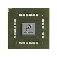
Manufacturer Part Number
MPC8544DS
Description
BOARD DEVELOPMENT SYSTEM 8544
Manufacturer
Freescale Semiconductor
Series
PowerQUICC III™r
Type
MPUr
Datasheets
1.MPC8544VTALF.pdf
(117 pages)
2.MPC8544VTALF.pdf
(2 pages)
3.MPC8544VTALF.pdf
(1340 pages)
4.MPC8544DS.pdf
(2 pages)
Specifications of MPC8544DS
Contents
Board
Processor To Be Evaluated
MPC8544E
Data Bus Width
32 bit
Interface Type
Ethernet, I2C
Operating Supply Voltage
- 0.3 V to + 1.1 V
Leaded Process Compatible
Yes
Peak Reflow Compatible (260 C)
Yes
Rohs Compliant
Yes
For Use With/related Products
MPC8544
For Use With
PPC8544EVTANG - EVAL MPC8544 783FCPBGA
Lead Free Status / RoHS Status
Lead free / RoHS Compliant


Enhanced Three-Speed Ethernet Controllers
15-190
Other information about the link is also returned. (Extend Status, No pre, Remote Fault, An Ability, Link status, extend
This advertises to the Link Partner that the TBI supports PAUSE and Full Duplex mode and does not support Half
This enables the TBI to restart Auto-Negotiations using the configuration set in the AN Advertisement register.
Set up the MII Mgmt for a read cycle to PHY MII Mgmt register (write the PHY address and Register address),
Set up the MII Mgmt for a write cycle to TBI’s AN Advertisement register (write the PHY address and Register
Set up the MII Mgmt for a write cycle to TBI’s Control register (write the PHY address and Register address),
The AN Advertisement register is at offset address 0x04 from the TBI’s address. (in this case 0x10)
MPC8544E PowerQUICC III Integrated Host Processor Family Reference Manual, Rev. 1
The PHY Status control register is at address 0x1 and in this case the PHY Address is 0x10.
Writing to MII Mgmt Control with 16-bit data intended for TBI’s AN Advertisement register,
the Control register is at offset address 0x00 from the TBI’s address. (in this case 0x10)
(Uses the PHY address (2) and Register address (2) placed in MIIMADD register),
Perform an MII Mgmt read cycle to verify state of TBI Control Register(0ptional)
Writing to MII Mgmt Control with 16-bit data intended for TBI’s Control register,
Table 15-156. TBI Mode Register Initialization Steps (continued)
(Uses the TBI address and Register address placed in MIIMADD register),
read the MIIMSTAT and look for AN Enable and other bit information.
MIIMSTAT ---> [0000_0000_0000_0000_0000_0000_0010_0000]
MIIMIND ---> [0000_0000_0000_0000_0000_0000_0000_0000]
MIIMIND ---> [0000_0000_0000_0000_0000_0000_0000_0000]
MIIMCON[0000_0000_0000_0000_0000_0001_1010_0000]
MIIMCON[0000_0000_0000_0000_0001_0010_0000_0000]
MIIMADD[0000_0000_0000_0000_0001_0000_0000_0100]
MIIMADD[0000_0000_0000_0000_0001_0000_0000_0000]
MIIMADD[0000_0000_0000_0000_0001_0000_0000_0001]
Read MII Mgmt Indicator register and check for Busy = 0,
Read MII Mgmt Indicator register and check for Busy = 0,
read the MIIMSTAT register and check bit 10 (AN Done)
Check to see if PHY has completed Auto-Negotiation.
Perform an MII Mgmt read cycle of Status Register.
This indicates that the write cycle was completed.
This indicates that the write cycle was completed.
Check to see if MII Mgmt write is complete.
Check to see if MII Mgmt write is complete.
Perform an MII Mgmt write cycle to TBI.
Perform an MII Mgmt write cycle to TBI.
Clear MIIMCOM[Read Cycle]
Clear MIIMCOM[Read Cycle]
Set MIIMCOM[Read Cycle]
Set MIIMCOM[Read Cycle]
When MIIMIND[BUSY]=0,
When MIIMIND[BUSY]=0,
Duplex mode.
address),
Ability)
Freescale Semiconductor
Related parts for MPC8544DS
Image
Part Number
Description
Manufacturer
Datasheet
Request
R

Part Number:
Description:
Manufacturer:
Freescale Semiconductor, Inc
Datasheet:
Part Number:
Description:
Manufacturer:
Freescale Semiconductor, Inc
Datasheet:
Part Number:
Description:
Manufacturer:
Freescale Semiconductor, Inc
Datasheet:
Part Number:
Description:
Manufacturer:
Freescale Semiconductor, Inc
Datasheet:
Part Number:
Description:
Manufacturer:
Freescale Semiconductor, Inc
Datasheet:
Part Number:
Description:
Manufacturer:
Freescale Semiconductor, Inc
Datasheet:
Part Number:
Description:
Manufacturer:
Freescale Semiconductor, Inc
Datasheet:
Part Number:
Description:
Manufacturer:
Freescale Semiconductor, Inc
Datasheet:
Part Number:
Description:
Manufacturer:
Freescale Semiconductor, Inc
Datasheet:
Part Number:
Description:
Manufacturer:
Freescale Semiconductor, Inc
Datasheet:
Part Number:
Description:
Manufacturer:
Freescale Semiconductor, Inc
Datasheet:
Part Number:
Description:
Manufacturer:
Freescale Semiconductor, Inc
Datasheet:
Part Number:
Description:
Manufacturer:
Freescale Semiconductor, Inc
Datasheet:
Part Number:
Description:
Manufacturer:
Freescale Semiconductor, Inc
Datasheet:
Part Number:
Description:
Manufacturer:
Freescale Semiconductor, Inc
Datasheet: