MPC8544DS Freescale Semiconductor, MPC8544DS Datasheet - Page 350
MPC8544DS
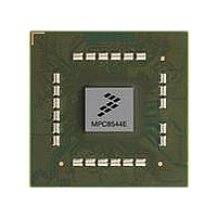
Manufacturer Part Number
MPC8544DS
Description
BOARD DEVELOPMENT SYSTEM 8544
Manufacturer
Freescale Semiconductor
Series
PowerQUICC III™r
Type
MPUr
Datasheets
1.MPC8544VTALF.pdf
(117 pages)
2.MPC8544VTALF.pdf
(2 pages)
3.MPC8544VTALF.pdf
(1340 pages)
4.MPC8544DS.pdf
(2 pages)
Specifications of MPC8544DS
Contents
Board
Processor To Be Evaluated
MPC8544E
Data Bus Width
32 bit
Interface Type
Ethernet, I2C
Operating Supply Voltage
- 0.3 V to + 1.1 V
Leaded Process Compatible
Yes
Peak Reflow Compatible (260 C)
Yes
Rohs Compliant
Yes
For Use With/related Products
MPC8544
For Use With
PPC8544EVTANG - EVAL MPC8544 783FCPBGA
Lead Free Status / RoHS Status
Lead free / RoHS Compliant


DDR Memory Controller
9.4.1.10
The DDR SDRAM mode 2 configuration register, shown in
DDR’s extended mode 2 and 3 registers (for DDR2).
Table 9-15
9.4.1.11
The DDR SDRAM mode control register, shown in
tasks:
Table 9-16
register to accomplish the above tasks.
9-26
Offset 0x120
Reset
16–31
0–15
Bits
W
•
•
•
•
R
Offset 0x11C
Reset
MD_EN — CS_SEL — MD_SEL SET_REF SET_PRE CKE_CNTL
W
Issue a mode register set command to a particular chip select
Issue an immediate refresh to a particular chip select
Issue an immediate precharge or precharge all command to a particular chip select
Force the CKE signals to a specific value
R
ESDMODE2 Extended SDRAM mode 2. Specifies the initial value loaded into the DDR SDRAM extended 2 mode
ESDMODE3 Extended SDRAM mode 3. Specifies the initial value loaded into the DDR SDRAM extended 3 mode
0
0
describes the DDR_SDRAM_MODE_2 fields.
describes the fields of this register.
Name
Figure 9-11. DDR SDRAM Mode 2 Configuration Register (DDR_SDRAM_MODE_2)
DDR SDRAM Mode 2 Configuration (DDR_SDRAM_MODE_2)
DDR SDRAM Mode Control Register (DDR_SDRAM_MD_CNTL)
1
MPC8544E PowerQUICC III Integrated Host Processor Family Reference Manual, Rev. 1
Figure 9-12. DDR SDRAM Mode Control Register (DDR_SDRAM_MD_CNTL)
2
register. The range and meaning of legal values is specified by the DDR SDRAM manufacturer.
When this value is driven onto the address bus (during the DDR SDRAM initialization sequence),
MA[0] presents the lsb bit of ESDMODE2, which, in the big-endian convention shown in
corresponds to ESDMODE2[15]. The msb of the SDRAM extended mode 2 register value must be
stored at ESDMODE2[0].
register. The range of legal values of legal values is specified by the DDR SDRAM manufacturer.
When this value is driven onto the address bus (during DDR SDRAM initialization), MA[0] presents the
lsb of ESDMODE3, which, in the big-endian convention shown in
ESDMODE3[15]. The msb of the SDRAM extended mode 3 register value must be stored at
ESDMODE3[0].
3
4
Table 9-15. DDR_SDRAM_MODE_2 Field Descriptions
5
ESDMODE2
7
8
Table 9-17
9
Figure
All zeros
All zeros
15 16
10
Description
shows the user how to set the fields of this
9-12, allows the user to carry out the following
Figure
11
12
9-11, sets the values loaded into the
—
13
ESDMODE3
Figure
15 16
9-11, corresponds to
Freescale Semiconductor
Access: Read/Write
MD_VALUE
Access: Read/Write
Figure
31
9-11,
31
Related parts for MPC8544DS
Image
Part Number
Description
Manufacturer
Datasheet
Request
R

Part Number:
Description:
Manufacturer:
Freescale Semiconductor, Inc
Datasheet:
Part Number:
Description:
Manufacturer:
Freescale Semiconductor, Inc
Datasheet:
Part Number:
Description:
Manufacturer:
Freescale Semiconductor, Inc
Datasheet:
Part Number:
Description:
Manufacturer:
Freescale Semiconductor, Inc
Datasheet:
Part Number:
Description:
Manufacturer:
Freescale Semiconductor, Inc
Datasheet:
Part Number:
Description:
Manufacturer:
Freescale Semiconductor, Inc
Datasheet:
Part Number:
Description:
Manufacturer:
Freescale Semiconductor, Inc
Datasheet:
Part Number:
Description:
Manufacturer:
Freescale Semiconductor, Inc
Datasheet:
Part Number:
Description:
Manufacturer:
Freescale Semiconductor, Inc
Datasheet:
Part Number:
Description:
Manufacturer:
Freescale Semiconductor, Inc
Datasheet:
Part Number:
Description:
Manufacturer:
Freescale Semiconductor, Inc
Datasheet:
Part Number:
Description:
Manufacturer:
Freescale Semiconductor, Inc
Datasheet:
Part Number:
Description:
Manufacturer:
Freescale Semiconductor, Inc
Datasheet:
Part Number:
Description:
Manufacturer:
Freescale Semiconductor, Inc
Datasheet:
Part Number:
Description:
Manufacturer:
Freescale Semiconductor, Inc
Datasheet: