MPC8544DS Freescale Semiconductor, MPC8544DS Datasheet - Page 305
MPC8544DS
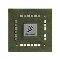
Manufacturer Part Number
MPC8544DS
Description
BOARD DEVELOPMENT SYSTEM 8544
Manufacturer
Freescale Semiconductor
Series
PowerQUICC III™r
Type
MPUr
Datasheets
1.MPC8544VTALF.pdf
(117 pages)
2.MPC8544VTALF.pdf
(2 pages)
3.MPC8544VTALF.pdf
(1340 pages)
4.MPC8544DS.pdf
(2 pages)
Specifications of MPC8544DS
Contents
Board
Processor To Be Evaluated
MPC8544E
Data Bus Width
32 bit
Interface Type
Ethernet, I2C
Operating Supply Voltage
- 0.3 V to + 1.1 V
Leaded Process Compatible
Yes
Peak Reflow Compatible (260 C)
Yes
Rohs Compliant
Yes
For Use With/related Products
MPC8544
For Use With
PPC8544EVTANG - EVAL MPC8544 783FCPBGA
Lead Free Status / RoHS Status
Lead free / RoHS Compliant


Table 7-26
7.9.5
Table 7-27
Core-initiated transactions caused when the core executes msync, mbar, tlbivax, or tlbsync do not change
the L2 cache state. The table does not list initial L1 states for transactions that hit in the L1 (iL1 or dL1)
and are not sent to the L2.
In the table, the heading ‘L2 hit’ indicates that the L2 provides (on a read) or captures (on a write) data for
an existing line. Some entries list two final L1 states. L2 touch instructions never allocate into iL1 or dL1.
Note that if the L2 SRAM is disabled, the L2 initial and final states are always I and the L2 never hits.
Similarly, if the L2 SRAM is in full memory-mapped SRAM mode, the L2 initial and final states are
always I and the L2 never hits for addresses not in the memory-mapped SRAM address range. The L2
always hits for addresses in the enabled memory-mapped SRAM address ranges.
Freescale Semiconductor
Cacheable instruction fetch
icbtls_L1
icbt_L2
•
•
Source of Transaction
Data locked (DL)
Stale (T)
shows L2 cache states. Note that these conventions are also used in
lists state transitions for all e500 core-initiated transactions that change the L2 cache state.
L2 State Transitions
MPC8544E PowerQUICC III Integrated Host Processor Family Reference Manual, Rev. 1
Table 7-27. State Transitions Due to Core-Initiated Transactions
V
0
1
1
1
1
1
1
1
1
Initial States
dL1
iL1
I,E
L1
I
T
0
0
0
0
1
1
1
1
x
IL
x
0
0
1
1
0
0
1
1
E/EL
I//T
L2
Table 7-26. L2 Cache States
T
I
DL
0
1
0
1
0
1
0
1
x
Yes
Invalid (I)
Exclusive (E)
Exclusive data locked (EDL)
Exclusive instruction locked (EIL)
Exclusive instruction and data locked (EL)
Stale (data invalid, locks invalid) (T)
Stale (data invalid, dlock valid) (TDL)
Stale (data invalid, ilock valid) (TIL)
Stale (data invalid, locks valid) (TL)
Hit
No
No
No
L2
Final States
I/V
I/V
I/V
I/V
L1
same L2CTL[L2DO] = 1. L2 touch instructions not
same
EL
L2
L2 states
E
allocated in L1
L2CTL[L2DO] = 0
L2CTL[L2DO] = 0. Restore locked line in L2 with
valid data from bus
Comments
Table
L2 Look-Aside Cache/SRAM
7-27.
7-35
Related parts for MPC8544DS
Image
Part Number
Description
Manufacturer
Datasheet
Request
R

Part Number:
Description:
Manufacturer:
Freescale Semiconductor, Inc
Datasheet:
Part Number:
Description:
Manufacturer:
Freescale Semiconductor, Inc
Datasheet:
Part Number:
Description:
Manufacturer:
Freescale Semiconductor, Inc
Datasheet:
Part Number:
Description:
Manufacturer:
Freescale Semiconductor, Inc
Datasheet:
Part Number:
Description:
Manufacturer:
Freescale Semiconductor, Inc
Datasheet:
Part Number:
Description:
Manufacturer:
Freescale Semiconductor, Inc
Datasheet:
Part Number:
Description:
Manufacturer:
Freescale Semiconductor, Inc
Datasheet:
Part Number:
Description:
Manufacturer:
Freescale Semiconductor, Inc
Datasheet:
Part Number:
Description:
Manufacturer:
Freescale Semiconductor, Inc
Datasheet:
Part Number:
Description:
Manufacturer:
Freescale Semiconductor, Inc
Datasheet:
Part Number:
Description:
Manufacturer:
Freescale Semiconductor, Inc
Datasheet:
Part Number:
Description:
Manufacturer:
Freescale Semiconductor, Inc
Datasheet:
Part Number:
Description:
Manufacturer:
Freescale Semiconductor, Inc
Datasheet:
Part Number:
Description:
Manufacturer:
Freescale Semiconductor, Inc
Datasheet:
Part Number:
Description:
Manufacturer:
Freescale Semiconductor, Inc
Datasheet: