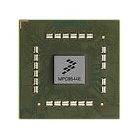
MPC8544DS Freescale Semiconductor, MPC8544DS Datasheet - Page 559

MPC8544DS
Manufacturer Part Number
MPC8544DS
Description
BOARD DEVELOPMENT SYSTEM 8544
Manufacturer
Freescale Semiconductor
Series
PowerQUICC III™r
Type
MPUr
Datasheets
1.MPC8544VTALF.pdf
(117 pages)
2.MPC8544VTALF.pdf
(2 pages)
3.MPC8544VTALF.pdf
(1340 pages)
4.MPC8544DS.pdf
(2 pages)
Specifications of MPC8544DS
Contents
Board
Processor To Be Evaluated
MPC8544E
Data Bus Width
32 bit
Interface Type
Ethernet, I2C
Operating Supply Voltage
- 0.3 V to + 1.1 V
Leaded Process Compatible
Yes
Peak Reflow Compatible (260 C)
Yes
Rohs Compliant
Yes
For Use With/related Products
MPC8544
For Use With
PPC8544EVTANG - EVAL MPC8544 783FCPBGA
Lead Free Status / RoHS Status
Lead free / RoHS Compliant
- MPC8544VTALF PDF datasheet
- MPC8544VTALF PDF datasheet #2
- MPC8544VTALF PDF datasheet #3
- MPC8544DS PDF datasheet #4
- Current page: 559 of 1340
- Download datasheet (12Mb)
12.4.6.9.5
The AESU key registers hold from 16, 24, or 32 bytes of key data, with the first 8 bytes of key data written
to key 1. Any key data written to bytes beyond the value written to the key size register is ignored. The
key data registers are cleared when the AESU is reset or re-initialized. If these registers are modified
during message processing, a context error is generated.
The key data registers may be read when changing context in decrypt mode. To resume processing, the
value read must be written back to the key registers and the restore decrypt key bit must be set in the mode
register. This eliminates the overhead of expanding the key prior to starting decryption when switching
context.
12.4.6.9.6
The AESU fetches data 128 bits at a time from the input FIFO. During processing, the input data is
encrypted or decrypted with the key and initialization vector (CBC mode only) and the results are placed
in the output FIFO. The output size is the same as the input size.
Writing to the FIFO address space places 64 bits of message data into the input FIFO. The input FIFO may
be written any time the number of dwords currently in the input FIFO (as indicated by the IFL field of the
AESU status register) is less than 32. There is no limit on the total number of bytes in a message. The
number of bits in the final message block must be set in the data size register.
Reading from the FIFO address space will pop 64 bits of message data from the output FIFO. The output
FIFO may be read any time the OFR signal is asserted (as indicated in the AESU status register). This
indicates that the number of bytes in the output FIFO is at or above the threshold specified in the mode
register.
12.4.7
This section contains details about the Kasumi execution unit (KEU), including modes of operation, status
and control registers, and FIFOs. The Kasumi execution unit (KEU) has been designed to support the F8
confidentiality function of the 3GPP, GSM A5/3, EDGE A5/3 and GPRS GEA3 algorithms and also the
3GPP F9 integrity function.
Most of the registers described here would not normally be accessed by the host. They are documented
here mainly for debug purposes. In typical operation, the KEU is used through channel-controlled access,
which means that most reads and writes of KEU registers are directed by the SEC channels. Driver
software performs host-controlled register accesses on only a few registers for initial configuration and
error handling.
Freescale Semiconductor
Kasumi Execution Unit (KEU)
MPC8544E PowerQUICC III Integrated Host Processor Family Reference Manual, Rev. 1
For both encrypt and decrypt operations, if the 802.11 frame is being
processed as a whole (not split across multiple descriptors), the initialize
and final MAC bits should be set in the AESU mode register.
AESU Key Registers
AESU FIFOs
NOTE
Security Engine (SEC) 2.1
12-79
Related parts for MPC8544DS
Image
Part Number
Description
Manufacturer
Datasheet
Request
R
Part Number:
Description:
Manufacturer:
Freescale Semiconductor, Inc
Datasheet:
Part Number:
Description:
Manufacturer:
Freescale Semiconductor, Inc
Datasheet:
Part Number:
Description:
Manufacturer:
Freescale Semiconductor, Inc
Datasheet:
Part Number:
Description:
Manufacturer:
Freescale Semiconductor, Inc
Datasheet:
Part Number:
Description:
Manufacturer:
Freescale Semiconductor, Inc
Datasheet:
Part Number:
Description:
Manufacturer:
Freescale Semiconductor, Inc
Datasheet:
Part Number:
Description:
Manufacturer:
Freescale Semiconductor, Inc
Datasheet:
Part Number:
Description:
Manufacturer:
Freescale Semiconductor, Inc
Datasheet:
Part Number:
Description:
Manufacturer:
Freescale Semiconductor, Inc
Datasheet:
Part Number:
Description:
Manufacturer:
Freescale Semiconductor, Inc
Datasheet:
Part Number:
Description:
Manufacturer:
Freescale Semiconductor, Inc
Datasheet:
Part Number:
Description:
Manufacturer:
Freescale Semiconductor, Inc
Datasheet:
Part Number:
Description:
Manufacturer:
Freescale Semiconductor, Inc
Datasheet:
Part Number:
Description:
Manufacturer:
Freescale Semiconductor, Inc
Datasheet:
Part Number:
Description:
Manufacturer:
Freescale Semiconductor, Inc
Datasheet:


