MPC8544DS Freescale Semiconductor, MPC8544DS Datasheet - Page 25
MPC8544DS
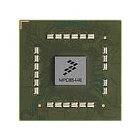
Manufacturer Part Number
MPC8544DS
Description
BOARD DEVELOPMENT SYSTEM 8544
Manufacturer
Freescale Semiconductor
Series
PowerQUICC III™r
Type
MPUr
Datasheets
1.MPC8544VTALF.pdf
(117 pages)
2.MPC8544VTALF.pdf
(2 pages)
3.MPC8544VTALF.pdf
(1340 pages)
4.MPC8544DS.pdf
(2 pages)
Specifications of MPC8544DS
Contents
Board
Processor To Be Evaluated
MPC8544E
Data Bus Width
32 bit
Interface Type
Ethernet, I2C
Operating Supply Voltage
- 0.3 V to + 1.1 V
Leaded Process Compatible
Yes
Peak Reflow Compatible (260 C)
Yes
Rohs Compliant
Yes
For Use With/related Products
MPC8544
For Use With
PPC8544EVTANG - EVAL MPC8544 783FCPBGA
Lead Free Status / RoHS Status
Lead free / RoHS Compliant


Paragraph
Number
14.4.2.4
14.4.3
14.4.3.1
14.4.3.2
14.4.3.3
14.4.3.4
14.4.3.5
14.4.3.6
14.4.3.7
14.4.3.7.1
14.4.3.7.2
14.4.3.7.3
14.4.3.7.4
14.4.3.7.5
14.4.3.7.6
14.4.3.8
14.4.3.9
14.4.3.10
14.4.3.11
14.4.3.11.1
14.4.4
14.4.4.1
14.4.4.1.1
14.4.4.1.2
14.4.4.1.3
14.4.4.1.4
14.4.4.2
14.4.4.2.1
14.4.4.2.2
14.4.4.3
14.4.4.4
14.4.4.4.1
14.4.4.4.2
14.4.4.4.3
14.4.4.4.4
14.4.4.4.5
14.4.4.4.6
14.4.4.4.7
14.4.4.4.8
Freescale Semiconductor
MPC8544E PowerQUICC III Integrated Host Processor Family Reference Manual, Rev. 1
SDRAM Machine .................................................................................................... 14-47
User-Programmable Machines (UPMs)................................................................... 14-58
Boot Chip-Select Operation................................................................................. 14-46
Supported SDRAM Configurations..................................................................... 14-47
SDRAM Power-On Initialization ........................................................................ 14-48
Intel PC133 and JEDEC-Standard SDRAM Interface Commands ..................... 14-49
Page Hit Checking ............................................................................................... 14-50
Page Management................................................................................................ 14-50
SDRAM Address Multiplexing ........................................................................... 14-50
SDRAM Device-Specific Parameters.................................................................. 14-51
SDRAM Interface Timing ................................................................................... 14-55
SDRAM Read/Write Transactions....................................................................... 14-57
SDRAM MODE-SET Command Timing............................................................ 14-57
SDRAM Refresh.................................................................................................. 14-57
UPM Requests ..................................................................................................... 14-59
Programming the UPMs ...................................................................................... 14-62
UPM Signal Timing............................................................................................. 14-64
RAM Array .......................................................................................................... 14-64
Precharge-to-Activate Interval......................................................................... 14-52
Activate-to-Read/Write Interval ...................................................................... 14-52
Column Address to First Data Out—CAS Latency......................................... 14-53
Last Data In to Precharge—Write Recovery ................................................... 14-53
Refresh Recovery Interval (RFRC) ................................................................. 14-54
External Address and Command Buffers (BUFCMD).................................... 14-54
SDRAM Refresh Timing ................................................................................. 14-58
Memory Access Requests................................................................................ 14-60
UPM Refresh Timer Requests ......................................................................... 14-61
Software Requests—RUN Command ............................................................. 14-61
Exception Requests.......................................................................................... 14-62
UPM Programming Example (Two Sequential Writes to the
UPM Programming Example (Two Sequential Reads from the
RAM Words..................................................................................................... 14-65
Chip-Select Signal Timing (CSTn) ................................................................. 14-67
Byte Select Signal Timing (BSTn) .................................................................. 14-68
General-Purpose Signals (GnTn, GOn)........................................................... 14-69
Loop Control (LOOP) ..................................................................................... 14-69
Repeat Execution of Current RAM Word (REDO) ......................................... 14-69
Address Multiplexing (AMX) ......................................................................... 14-70
Data Valid and Data Sample Control (UTA) ................................................... 14-71
RAM Array) ................................................................................................ 14-63
RAM Array) ................................................................................................ 14-63
Contents
Title
Number
Page
xxv
Related parts for MPC8544DS
Image
Part Number
Description
Manufacturer
Datasheet
Request
R

Part Number:
Description:
Manufacturer:
Freescale Semiconductor, Inc
Datasheet:
Part Number:
Description:
Manufacturer:
Freescale Semiconductor, Inc
Datasheet:
Part Number:
Description:
Manufacturer:
Freescale Semiconductor, Inc
Datasheet:
Part Number:
Description:
Manufacturer:
Freescale Semiconductor, Inc
Datasheet:
Part Number:
Description:
Manufacturer:
Freescale Semiconductor, Inc
Datasheet:
Part Number:
Description:
Manufacturer:
Freescale Semiconductor, Inc
Datasheet:
Part Number:
Description:
Manufacturer:
Freescale Semiconductor, Inc
Datasheet:
Part Number:
Description:
Manufacturer:
Freescale Semiconductor, Inc
Datasheet:
Part Number:
Description:
Manufacturer:
Freescale Semiconductor, Inc
Datasheet:
Part Number:
Description:
Manufacturer:
Freescale Semiconductor, Inc
Datasheet:
Part Number:
Description:
Manufacturer:
Freescale Semiconductor, Inc
Datasheet:
Part Number:
Description:
Manufacturer:
Freescale Semiconductor, Inc
Datasheet:
Part Number:
Description:
Manufacturer:
Freescale Semiconductor, Inc
Datasheet:
Part Number:
Description:
Manufacturer:
Freescale Semiconductor, Inc
Datasheet:
Part Number:
Description:
Manufacturer:
Freescale Semiconductor, Inc
Datasheet: