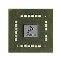
MPC8544DS Freescale Semiconductor, MPC8544DS Datasheet - Page 135

MPC8544DS
Manufacturer Part Number
MPC8544DS
Description
BOARD DEVELOPMENT SYSTEM 8544
Manufacturer
Freescale Semiconductor
Series
PowerQUICC III™r
Type
MPUr
Datasheets
1.MPC8544VTALF.pdf
(117 pages)
2.MPC8544VTALF.pdf
(2 pages)
3.MPC8544VTALF.pdf
(1340 pages)
4.MPC8544DS.pdf
(2 pages)
Specifications of MPC8544DS
Contents
Board
Processor To Be Evaluated
MPC8544E
Data Bus Width
32 bit
Interface Type
Ethernet, I2C
Operating Supply Voltage
- 0.3 V to + 1.1 V
Leaded Process Compatible
Yes
Peak Reflow Compatible (260 C)
Yes
Rohs Compliant
Yes
For Use With/related Products
MPC8544
For Use With
PPC8544EVTANG - EVAL MPC8544 783FCPBGA
Lead Free Status / RoHS Status
Lead free / RoHS Compliant
- MPC8544VTALF PDF datasheet
- MPC8544VTALF PDF datasheet #2
- MPC8544VTALF PDF datasheet #3
- MPC8544DS PDF datasheet #4
- Current page: 135 of 1340
- Download datasheet (12Mb)
In addition, many configuration registers affect accesses to other memory regions; therefore writes to these
registers must be guaranteed to have taken effect before accesses are made to the associated memory
regions.
To guarantee that the results of any sequence of writes to configuration registers are in effect, the final
configuration register write should be chased by a read of the same register, and that should be followed
by a SYNC instruction. Then accesses can safely be made to memory regions affected by the configuration
register write.
2.3.2
In addition to being accessible by the e500 processor, the configuration, control, and status registers are
accessible from external interfaces. This allows external masters on the I/O ports to configure the
MPC8544E.
External masters do not need to know the location of the CCSR memory in the local address map. Rather, they
access this region of the local memory map through a window defined by a register in the interface
programming model that is accessible to the external master from its external memory map.
The PCI base address for accessing the local CCSR memory is selectable through the PCI configuration
and status register base address register (PCSRBAR), at offset 0x10, described in
Base Address Registers.”
to the MPC8544E. Subsequent memory accesses by a PCI master to the PCI address range indicated by
PCSRBAR are translated to the local address indicated by the current setting of CCSRBAR.
2.3.3
The configuration, control, and status registers of the MPC8544E are grouped according to functional
units. Most functional blocks are allocated a 4-Kbyte address space for registers. Registers that fall into
this category are referred to as general utilities registers. These registers occupy the first 256 Kbytes of
CCSR memory.
Registers controlling functions that are not particular to a functional unit but to the device as a whole occupy
the highest 256 Kbytes of CCSR memory and are referred to as device-specific registers.
Some functional units, such as the OpenPIC-based interrupt controller have larger address spaces as
defined by their programming models. The registers for these blocks are given their own large regions of
CCSR memory.
Freescale Semiconductor
Accessing CCSR Memory from External Masters
Organization of CCSR Memory
Table 2-10. Local Memory Configuration, Control, and Status Register Summary
MPC8544E PowerQUICC III Integrated Host Processor Family Reference Manual, Rev. 1
Offset from CCSRBAR
0xC_0000–0xD_FFFF
0xE_0000–0xF_FFFF
0x8_0000–0xB_FFFF
0x0_0000–0x3_FFFF
0x4_0000–0x7_FFFF
An external PCI master sets this register by running a PCI configuration cycle
General utilities
Programmable interrupt controller (PIC)
Reserved
Reserved
Device-specific utilities
Register Grouping
Section 17.3.2.11, “PCI
Memory Map
2-11
Related parts for MPC8544DS
Image
Part Number
Description
Manufacturer
Datasheet
Request
R
Part Number:
Description:
Manufacturer:
Freescale Semiconductor, Inc
Datasheet:
Part Number:
Description:
Manufacturer:
Freescale Semiconductor, Inc
Datasheet:
Part Number:
Description:
Manufacturer:
Freescale Semiconductor, Inc
Datasheet:
Part Number:
Description:
Manufacturer:
Freescale Semiconductor, Inc
Datasheet:
Part Number:
Description:
Manufacturer:
Freescale Semiconductor, Inc
Datasheet:
Part Number:
Description:
Manufacturer:
Freescale Semiconductor, Inc
Datasheet:
Part Number:
Description:
Manufacturer:
Freescale Semiconductor, Inc
Datasheet:
Part Number:
Description:
Manufacturer:
Freescale Semiconductor, Inc
Datasheet:
Part Number:
Description:
Manufacturer:
Freescale Semiconductor, Inc
Datasheet:
Part Number:
Description:
Manufacturer:
Freescale Semiconductor, Inc
Datasheet:
Part Number:
Description:
Manufacturer:
Freescale Semiconductor, Inc
Datasheet:
Part Number:
Description:
Manufacturer:
Freescale Semiconductor, Inc
Datasheet:
Part Number:
Description:
Manufacturer:
Freescale Semiconductor, Inc
Datasheet:
Part Number:
Description:
Manufacturer:
Freescale Semiconductor, Inc
Datasheet:
Part Number:
Description:
Manufacturer:
Freescale Semiconductor, Inc
Datasheet:


