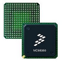
MC68EN360CAI25L Freescale Semiconductor, MC68EN360CAI25L Datasheet - Page 809

MC68EN360CAI25L
Manufacturer Part Number
MC68EN360CAI25L
Description
IC MPU QUICC 25MHZ 240-FQFP
Manufacturer
Freescale Semiconductor
Series
MC68000r
Datasheets
1.MC68EN302AG20BT.pdf
(8 pages)
2.MC68EN360VR25L.pdf
(14 pages)
3.MC68EN360VR25L.pdf
(2 pages)
4.MC68EN360CAI25L.pdf
(962 pages)
Specifications of MC68EN360CAI25L
Processor Type
M683xx 32-Bit
Speed
25MHz
Voltage
5V
Mounting Type
Surface Mount
Package / Case
240-FQFP
Core Size
32 Bit
Cpu Speed
25MHz
Embedded Interface Type
SCP, TDM
Digital Ic Case Style
FQFP
No. Of Pins
240
Supply Voltage Range
4.75V To 5.25V
Rohs Compliant
Yes
Family Name
M68xxx
Device Core
ColdFire
Device Core Size
32b
Frequency (max)
25MHz
Instruction Set Architecture
RISC
Supply Voltage 1 (typ)
5V
Operating Supply Voltage (max)
5.25V
Operating Supply Voltage (min)
4.75V
Operating Temp Range
-40C to 85C
Operating Temperature Classification
Industrial
Mounting
Surface Mount
Pin Count
240
Package Type
FQFP
Lead Free Status / RoHS Status
Lead free / RoHS Compliant
Features
-
Lead Free Status / Rohs Status
Compliant
Available stocks
Company
Part Number
Manufacturer
Quantity
Price
Company:
Part Number:
MC68EN360CAI25L
Manufacturer:
APLHA
Quantity:
12 000
Company:
Part Number:
MC68EN360CAI25L
Manufacturer:
Freescale Semiconductor
Quantity:
10 000
Part Number:
MC68EN360CAI25L
Manufacturer:
FREESCALE
Quantity:
20 000
- MC68EN302AG20BT PDF datasheet
- MC68EN360VR25L PDF datasheet #2
- MC68EN360VR25L PDF datasheet #3
- MC68EN360CAI25L PDF datasheet #4
- Current page: 809 of 962
- Download datasheet (4Mb)
Applications
9.8.4 Interfacing Multiple QUICCs to an MC68EC030
It is possible to interface multiple QUICCs to an MC68EC030. The first QUICC can be con-
figured as previously shown in this subsection. Additional QUICCs should be configured as
noted in the following list:
9.8.5 Using a Higher Speed MC68EC030 Master with the QUICC
It is possible to interface an MC68EC030 and QUICC through an asynchronous bus. This
should allow an external master to operate at higher frequencies than those of the QUICC
with minimal effort. As of this writing, the QUICC top frequency is 25 MHz; whereas,
MC68EC030s are available up to 40 MHz. One potentially attractive option for a designer
would be to consider disabling the CPU32+ core and increasing system performance by
adding a 40-MHz MC68EC030 asynchronously. While this option is available, it is important
for the designer to consider what effects a higher speed MC68EC030 would ultimately have
on system cost and performance over using the QUICC CPU32+ at a lower frequency.
For the designer to take full advantage of a high-speed MC68EC030, it will be necessary to
add additional glue to that shown in Figure 9-27. The additional circuitry takes the form of a
DRAM controller, which is used instead of using the QUICC memory controller. The need
for the additional logic is twofold. First, if the QUICC memory controller capabilities are used,
all memory accesses would be at the clock rate of 25 MHz. In addition, since the
9-89
The AM27–AM11 bits should be programmed to determine the block size of the chip se-
lect or RASx line. This should be the total number of bytes in each memory array except
for the EEPROM, which should be 32 Kbytes, rather than 8 Kbytes.
FCM3–FCM0 may be set to all ones to allow the chip select or RASx line to assert on all
function codes except CPU space (interrupt acknowledge). It is advisable to program
FCM3–FCM0 to ones, at least during the initial stages of debugging.
BCYC1–BCYC0 is not applicable.
PGME should be set to enable page mode and cleared otherwise.
SPS1–SPS0 should be cleared (32-bit SRAM port).
DSSEL should be set only if this is a DRAM bank.
• The additional QUICCs should have their CONFIG2–CONFIG0 pins configured for
• The MBAR of the additional QUICCs should be programmed using the MBARE pin and
• An external bus arbiter is required to take the bus request of the additional QUICC
• An external interrupt prioritizer is required to determine which QUICC IOUT2–IOUT0
slave mode, global chip select disabled , and MBAR at $003FF04.
MBARE register as described in the Section 6 System Integration Module (SIM60).
(which is an output because of the CONFIG2–CONFIG0 pins) and prioritize it with the
other QUICCs, present it to the MC68EC030, and issue a bus grant to the appropriate
QUICC.
pins are currently routed to the MC68EC030. Alternatively, the additional QUICC
should have its interrupts brought out on a single RQOUT pin, which is routed to one of
the original QUICC interrupt inputs. This would eliminate the external logic.
Freescale Semiconductor, Inc.
For More Information On This Product,
MC68360 USER’S MANUAL
Go to: www.freescale.com
Related parts for MC68EN360CAI25L
Image
Part Number
Description
Manufacturer
Datasheet
Request
R
Part Number:
Description:
Manufacturer:
Freescale Semiconductor, Inc
Datasheet:
Part Number:
Description:
Manufacturer:
Freescale Semiconductor, Inc
Datasheet:
Part Number:
Description:
Manufacturer:
Freescale Semiconductor, Inc
Datasheet:
Part Number:
Description:
Manufacturer:
Freescale Semiconductor, Inc
Datasheet:
Part Number:
Description:
Manufacturer:
Freescale Semiconductor, Inc
Datasheet:
Part Number:
Description:
Manufacturer:
Freescale Semiconductor, Inc
Datasheet:
Part Number:
Description:
Manufacturer:
Freescale Semiconductor, Inc
Datasheet:
Part Number:
Description:
Manufacturer:
Freescale Semiconductor, Inc
Datasheet:
Part Number:
Description:
Manufacturer:
Freescale Semiconductor, Inc
Datasheet:
Part Number:
Description:
Manufacturer:
Freescale Semiconductor, Inc
Datasheet:
Part Number:
Description:
Manufacturer:
Freescale Semiconductor, Inc
Datasheet:
Part Number:
Description:
Manufacturer:
Freescale Semiconductor, Inc
Datasheet:
Part Number:
Description:
Manufacturer:
Freescale Semiconductor, Inc
Datasheet:
Part Number:
Description:
Manufacturer:
Freescale Semiconductor, Inc
Datasheet:
Part Number:
Description:
Manufacturer:
Freescale Semiconductor, Inc
Datasheet:


