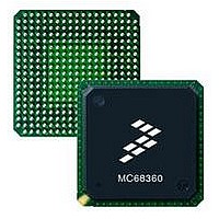
MC68EN360CAI25L Freescale Semiconductor, MC68EN360CAI25L Datasheet - Page 286

MC68EN360CAI25L
Manufacturer Part Number
MC68EN360CAI25L
Description
IC MPU QUICC 25MHZ 240-FQFP
Manufacturer
Freescale Semiconductor
Series
MC68000r
Datasheets
1.MC68EN302AG20BT.pdf
(8 pages)
2.MC68EN360VR25L.pdf
(14 pages)
3.MC68EN360VR25L.pdf
(2 pages)
4.MC68EN360CAI25L.pdf
(962 pages)
Specifications of MC68EN360CAI25L
Processor Type
M683xx 32-Bit
Speed
25MHz
Voltage
5V
Mounting Type
Surface Mount
Package / Case
240-FQFP
Core Size
32 Bit
Cpu Speed
25MHz
Embedded Interface Type
SCP, TDM
Digital Ic Case Style
FQFP
No. Of Pins
240
Supply Voltage Range
4.75V To 5.25V
Rohs Compliant
Yes
Family Name
M68xxx
Device Core
ColdFire
Device Core Size
32b
Frequency (max)
25MHz
Instruction Set Architecture
RISC
Supply Voltage 1 (typ)
5V
Operating Supply Voltage (max)
5.25V
Operating Supply Voltage (min)
4.75V
Operating Temp Range
-40C to 85C
Operating Temperature Classification
Industrial
Mounting
Surface Mount
Pin Count
240
Package Type
FQFP
Lead Free Status / RoHS Status
Lead free / RoHS Compliant
Features
-
Lead Free Status / Rohs Status
Compliant
Available stocks
Company
Part Number
Manufacturer
Quantity
Price
Company:
Part Number:
MC68EN360CAI25L
Manufacturer:
APLHA
Quantity:
12 000
Company:
Part Number:
MC68EN360CAI25L
Manufacturer:
Freescale Semiconductor
Quantity:
10 000
Part Number:
MC68EN360CAI25L
Manufacturer:
FREESCALE
Quantity:
20 000
- MC68EN302AG20BT PDF datasheet
- MC68EN360VR25L PDF datasheet #2
- MC68EN360VR25L PDF datasheet #3
- MC68EN360CAI25L PDF datasheet #4
- Current page: 286 of 962
- Download datasheet (4Mb)
System Integration Module (SIM60)
tial general system clock of 13.14 MHz. The user would then write the MF bits to raise this
frequency to the desired frequency.
6.9.3.11 CLOCK DIVIDER CONTROL REGISTER (CDVCR). The CDVCR controls the
operation of the low-power divider for the various clocks on the QUICC. It can be read or
written only in supervisor mode. Writing this register is allowed only if the CDVWP bit is zero.
The reset state of CDVCR produces the maximum frequency for all the clocks that it affects.
CDVWP—CDVCR Write Protect
DFSY—Division Factor for the SyncCLK
DFTM—Division Factor for the BRGCLK
INTEN—Interrupt Enable
6-42
CDVWP
This bit protects accidental writing of the CDVCR. After reset, this bit defaults to zero to
enable writing. Setting this bit prevents further writing (excluding the first write that sets
this bit).
These bits define the SyncCLK frequency. Changing the value of the these bits will not
result in a loss-of-lock condition. These bits are cleared by a hardware reset. The default
value is divide by 1 (VCO/2) which is 25 MHz in a 25-MHz system.
These bits define the BRGCLK frequency. Changing the value of the these bits will not
result in a loss-of-lock condition. These bits are cleared by a hardware reset. The default
value is divide by 1 (VCO/2) which is 25 MHz in a 25-MHz system.
These bits specify if the general system clock returns to high frequency (defined by the
DFNH bits) while the CPU32+ either has a pending interrupt or an interrupt routine in pro-
cess, either of which has a level higher than INTEN2–INTEN0. To prevent interrupts from
causing the general system clock to automatically switch to high frequency, write INTEN
with 111.
15
0
00 = Divide by 1 (normal operation)
01 = Divide by 4
10 = Divide by 16
11 = Divide by 64
00 = Divide by 1 (normal operation)
01 = Divide by 4
10 = Divide by 16
11 = Divide by 64
14
0
DFSY
SWT clocking does not stop when the PLL is in the process of
acquiring a lock. Therefore, the user should service the SWT (re-
set its count) before and after changing the MF bits.
13
0
12
0
DFTM
Freescale Semiconductor, Inc.
11
0
For More Information On This Product,
10
0
MC68360 USER’S MANUAL
Go to: www.freescale.com
INTEN
9
0
NOTE
8
0
RRQEN
0
7
6
0
DFNL
5
0
4
0
3
0
DFNH
0
2
1
0
CSRC
0
0
Related parts for MC68EN360CAI25L
Image
Part Number
Description
Manufacturer
Datasheet
Request
R
Part Number:
Description:
Manufacturer:
Freescale Semiconductor, Inc
Datasheet:
Part Number:
Description:
Manufacturer:
Freescale Semiconductor, Inc
Datasheet:
Part Number:
Description:
Manufacturer:
Freescale Semiconductor, Inc
Datasheet:
Part Number:
Description:
Manufacturer:
Freescale Semiconductor, Inc
Datasheet:
Part Number:
Description:
Manufacturer:
Freescale Semiconductor, Inc
Datasheet:
Part Number:
Description:
Manufacturer:
Freescale Semiconductor, Inc
Datasheet:
Part Number:
Description:
Manufacturer:
Freescale Semiconductor, Inc
Datasheet:
Part Number:
Description:
Manufacturer:
Freescale Semiconductor, Inc
Datasheet:
Part Number:
Description:
Manufacturer:
Freescale Semiconductor, Inc
Datasheet:
Part Number:
Description:
Manufacturer:
Freescale Semiconductor, Inc
Datasheet:
Part Number:
Description:
Manufacturer:
Freescale Semiconductor, Inc
Datasheet:
Part Number:
Description:
Manufacturer:
Freescale Semiconductor, Inc
Datasheet:
Part Number:
Description:
Manufacturer:
Freescale Semiconductor, Inc
Datasheet:
Part Number:
Description:
Manufacturer:
Freescale Semiconductor, Inc
Datasheet:
Part Number:
Description:
Manufacturer:
Freescale Semiconductor, Inc
Datasheet:


