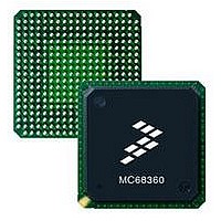
MC68EN360CAI25L Freescale Semiconductor, MC68EN360CAI25L Datasheet - Page 333

MC68EN360CAI25L
Manufacturer Part Number
MC68EN360CAI25L
Description
IC MPU QUICC 25MHZ 240-FQFP
Manufacturer
Freescale Semiconductor
Series
MC68000r
Datasheets
1.MC68EN302AG20BT.pdf
(8 pages)
2.MC68EN360VR25L.pdf
(14 pages)
3.MC68EN360VR25L.pdf
(2 pages)
4.MC68EN360CAI25L.pdf
(962 pages)
Specifications of MC68EN360CAI25L
Processor Type
M683xx 32-Bit
Speed
25MHz
Voltage
5V
Mounting Type
Surface Mount
Package / Case
240-FQFP
Core Size
32 Bit
Cpu Speed
25MHz
Embedded Interface Type
SCP, TDM
Digital Ic Case Style
FQFP
No. Of Pins
240
Supply Voltage Range
4.75V To 5.25V
Rohs Compliant
Yes
Family Name
M68xxx
Device Core
ColdFire
Device Core Size
32b
Frequency (max)
25MHz
Instruction Set Architecture
RISC
Supply Voltage 1 (typ)
5V
Operating Supply Voltage (max)
5.25V
Operating Supply Voltage (min)
4.75V
Operating Temp Range
-40C to 85C
Operating Temperature Classification
Industrial
Mounting
Surface Mount
Pin Count
240
Package Type
FQFP
Lead Free Status / RoHS Status
Lead free / RoHS Compliant
Features
-
Lead Free Status / Rohs Status
Compliant
Available stocks
Company
Part Number
Manufacturer
Quantity
Price
Company:
Part Number:
MC68EN360CAI25L
Manufacturer:
APLHA
Quantity:
12 000
Company:
Part Number:
MC68EN360CAI25L
Manufacturer:
Freescale Semiconductor
Quantity:
10 000
Part Number:
MC68EN360CAI25L
Manufacturer:
FREESCALE
Quantity:
20 000
- MC68EN302AG20BT PDF datasheet
- MC68EN360VR25L PDF datasheet #2
- MC68EN360VR25L PDF datasheet #3
- MC68EN360CAI25L PDF datasheet #4
- Current page: 333 of 962
- Download datasheet (4Mb)
The dual-port RAM can be accessed by the RISC or one of four bus masters: CPU32+ core,
IDMAs, SDMAs, or external bus master. When the dual-port RAM is accessed by an exter-
nal bus master, CPU32+ core, IDMA, or SDMA channel, it is accessed in three clocks. When
the dual-port RAM is accessed by the RISC, it is accessed in one clock. In the case of simul-
taneous access (with at least one write operation), the RISC is delayed by one clock.
When the dual-port RAM is accessed by the CPU32+ core, IDMAs, SDMAs, or external bus
master, the data and address are taken from the IMB. The data is then presented on the IMB
data bus. The RISC has access to the entire dual-port RAM for data fetches and portions of
the system RAM for microcode instruction fetches.
The dual-port RAM is used for five possible tasks; any two tasks can occur simultaneously.
The first use is to store parameters associated with the SCCs, SMCs, SPI, and IDMAs in the
768-byte parameter RAM. The second use is to store the buffer descriptors that describe
where data is to be received and transmitted from. The third use is to store data from the
serial channels. This usage is optional since data may also be stored externally in the sys-
tem memory. The fourth use is to store RAM microcode for the RISC processor. This feature
allows additional protocols to be added by Motorola in the future. The fifth use is for addi-
tional scratchpad RAM space for the user program.
PERIPHERAL
CP MICROCODE
INTERNAL
ADDRESS
ADDRESS
ADDRESS
BUS
IMB
Figure 7-3. Dual-Port RAM Block Diagram
Freescale Semiconductor, Inc.
For More Information On This Product,
MC68360 USER’S MANUAL
Go to: www.freescale.com
1792 BYTES
PARMETER
768 BYTES
SYSTEM
BYTES
BYTES
BYTES
BYTES
RAM
RAM
512
512
512
256
CP MICROCODE DATA
PERIPHERAL
DATA BUS
DATA BUS
IMB
Dual-Port RAM
Related parts for MC68EN360CAI25L
Image
Part Number
Description
Manufacturer
Datasheet
Request
R
Part Number:
Description:
Manufacturer:
Freescale Semiconductor, Inc
Datasheet:
Part Number:
Description:
Manufacturer:
Freescale Semiconductor, Inc
Datasheet:
Part Number:
Description:
Manufacturer:
Freescale Semiconductor, Inc
Datasheet:
Part Number:
Description:
Manufacturer:
Freescale Semiconductor, Inc
Datasheet:
Part Number:
Description:
Manufacturer:
Freescale Semiconductor, Inc
Datasheet:
Part Number:
Description:
Manufacturer:
Freescale Semiconductor, Inc
Datasheet:
Part Number:
Description:
Manufacturer:
Freescale Semiconductor, Inc
Datasheet:
Part Number:
Description:
Manufacturer:
Freescale Semiconductor, Inc
Datasheet:
Part Number:
Description:
Manufacturer:
Freescale Semiconductor, Inc
Datasheet:
Part Number:
Description:
Manufacturer:
Freescale Semiconductor, Inc
Datasheet:
Part Number:
Description:
Manufacturer:
Freescale Semiconductor, Inc
Datasheet:
Part Number:
Description:
Manufacturer:
Freescale Semiconductor, Inc
Datasheet:
Part Number:
Description:
Manufacturer:
Freescale Semiconductor, Inc
Datasheet:
Part Number:
Description:
Manufacturer:
Freescale Semiconductor, Inc
Datasheet:
Part Number:
Description:
Manufacturer:
Freescale Semiconductor, Inc
Datasheet:


