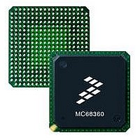
MC68EN360CAI25L Freescale Semiconductor, MC68EN360CAI25L Datasheet - Page 804

MC68EN360CAI25L
Manufacturer Part Number
MC68EN360CAI25L
Description
IC MPU QUICC 25MHZ 240-FQFP
Manufacturer
Freescale Semiconductor
Series
MC68000r
Datasheets
1.MC68EN302AG20BT.pdf
(8 pages)
2.MC68EN360VR25L.pdf
(14 pages)
3.MC68EN360VR25L.pdf
(2 pages)
4.MC68EN360CAI25L.pdf
(962 pages)
Specifications of MC68EN360CAI25L
Processor Type
M683xx 32-Bit
Speed
25MHz
Voltage
5V
Mounting Type
Surface Mount
Package / Case
240-FQFP
Core Size
32 Bit
Cpu Speed
25MHz
Embedded Interface Type
SCP, TDM
Digital Ic Case Style
FQFP
No. Of Pins
240
Supply Voltage Range
4.75V To 5.25V
Rohs Compliant
Yes
Family Name
M68xxx
Device Core
ColdFire
Device Core Size
32b
Frequency (max)
25MHz
Instruction Set Architecture
RISC
Supply Voltage 1 (typ)
5V
Operating Supply Voltage (max)
5.25V
Operating Supply Voltage (min)
4.75V
Operating Temp Range
-40C to 85C
Operating Temperature Classification
Industrial
Mounting
Surface Mount
Pin Count
240
Package Type
FQFP
Lead Free Status / RoHS Status
Lead free / RoHS Compliant
Features
-
Lead Free Status / Rohs Status
Compliant
Available stocks
Company
Part Number
Manufacturer
Quantity
Price
Company:
Part Number:
MC68EN360CAI25L
Manufacturer:
APLHA
Quantity:
12 000
Company:
Part Number:
MC68EN360CAI25L
Manufacturer:
Freescale Semiconductor
Quantity:
10 000
Part Number:
MC68EN360CAI25L
Manufacturer:
FREESCALE
Quantity:
20 000
- MC68EN302AG20BT PDF datasheet
- MC68EN360VR25L PDF datasheet #2
- MC68EN360VR25L PDF datasheet #3
- MC68EN360CAI25L PDF datasheet #4
- Current page: 804 of 962
- Download datasheet (4Mb)
Applications
9.8.2.4 EEPROM. Figure 9-31 shows the interface to an EEPROM device to give a small
amount of nonvolatile storage. In this case a byte-wide EEPROM bank is defined to mini-
mize cost. If the port size of the chip select is selected to be 8-bits, then each byte of the
EEPROM may be accessed in succession. The CS4 pin should be programmed to respond
to an 8K byte area in this design.
Only one byte should be written at a time. After a write is made, software is responsible for
waiting the appropriate time (e.g. 10 ms) or for doing data polling to see if the newly written
data byte is correct.
9.8.2.5 DRAM SIMM. Figure 9-32 shows the interface to an MCM32100S DRAM single in-
line memory module (SIMM). Both the MC68EC030 and the QUICC can access the DRAM.
When the QUICC is a slave to an external MC68EC030, the address multiplexing for the
DRAM must be done externally to the QUICC, which is accomplished in the three F157 mul-
tiplexers. The external address multiplexing scheme is very simple and allows page mode
operation to be provided for the MC68EC030, if desired. This multiplexing scheme exter-
nally provides, the same multiplexing method that the QUICC implements internally.
9-84
This multiplexing scheme allows the use of page mode, but re-
quires hardware modification if larger SIMMs are to be used on
the board. If the user is interested in the latter, rather than the
Figure 9-31. 8-Kbyte EEPROM Bank—8 Bits Wide
WE3
A12–A0
SYSTEM BUS AND
QUICC-GENERATED SIGNALS
R/W
D31–D24
CS4
Freescale Semiconductor, Inc.
For More Information On This Product,
MC68360 USER’S MANUAL
Go to: www.freescale.com
NOTE
DQ0
DQ1
DQ2
DQ3
DQ4
DQ5
DQ6
DQ7
CE (Enable)
OE
WE (Write)
EEPROM
PORT SIZE
8K 8
2864
BYTE
A10
A11
A12
A0
A2
A3
A4
A5
A6
A7
A8
A9
A1
Related parts for MC68EN360CAI25L
Image
Part Number
Description
Manufacturer
Datasheet
Request
R
Part Number:
Description:
Manufacturer:
Freescale Semiconductor, Inc
Datasheet:
Part Number:
Description:
Manufacturer:
Freescale Semiconductor, Inc
Datasheet:
Part Number:
Description:
Manufacturer:
Freescale Semiconductor, Inc
Datasheet:
Part Number:
Description:
Manufacturer:
Freescale Semiconductor, Inc
Datasheet:
Part Number:
Description:
Manufacturer:
Freescale Semiconductor, Inc
Datasheet:
Part Number:
Description:
Manufacturer:
Freescale Semiconductor, Inc
Datasheet:
Part Number:
Description:
Manufacturer:
Freescale Semiconductor, Inc
Datasheet:
Part Number:
Description:
Manufacturer:
Freescale Semiconductor, Inc
Datasheet:
Part Number:
Description:
Manufacturer:
Freescale Semiconductor, Inc
Datasheet:
Part Number:
Description:
Manufacturer:
Freescale Semiconductor, Inc
Datasheet:
Part Number:
Description:
Manufacturer:
Freescale Semiconductor, Inc
Datasheet:
Part Number:
Description:
Manufacturer:
Freescale Semiconductor, Inc
Datasheet:
Part Number:
Description:
Manufacturer:
Freescale Semiconductor, Inc
Datasheet:
Part Number:
Description:
Manufacturer:
Freescale Semiconductor, Inc
Datasheet:
Part Number:
Description:
Manufacturer:
Freescale Semiconductor, Inc
Datasheet:


