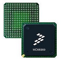
MC68EN360CAI25L Freescale Semiconductor, MC68EN360CAI25L Datasheet - Page 78

MC68EN360CAI25L
Manufacturer Part Number
MC68EN360CAI25L
Description
IC MPU QUICC 25MHZ 240-FQFP
Manufacturer
Freescale Semiconductor
Series
MC68000r
Datasheets
1.MC68EN302AG20BT.pdf
(8 pages)
2.MC68EN360VR25L.pdf
(14 pages)
3.MC68EN360VR25L.pdf
(2 pages)
4.MC68EN360CAI25L.pdf
(962 pages)
Specifications of MC68EN360CAI25L
Processor Type
M683xx 32-Bit
Speed
25MHz
Voltage
5V
Mounting Type
Surface Mount
Package / Case
240-FQFP
Core Size
32 Bit
Cpu Speed
25MHz
Embedded Interface Type
SCP, TDM
Digital Ic Case Style
FQFP
No. Of Pins
240
Supply Voltage Range
4.75V To 5.25V
Rohs Compliant
Yes
Family Name
M68xxx
Device Core
ColdFire
Device Core Size
32b
Frequency (max)
25MHz
Instruction Set Architecture
RISC
Supply Voltage 1 (typ)
5V
Operating Supply Voltage (max)
5.25V
Operating Supply Voltage (min)
4.75V
Operating Temp Range
-40C to 85C
Operating Temperature Classification
Industrial
Mounting
Surface Mount
Pin Count
240
Package Type
FQFP
Lead Free Status / RoHS Status
Lead free / RoHS Compliant
Features
-
Lead Free Status / Rohs Status
Compliant
Available stocks
Company
Part Number
Manufacturer
Quantity
Price
Company:
Part Number:
MC68EN360CAI25L
Manufacturer:
APLHA
Quantity:
12 000
Company:
Part Number:
MC68EN360CAI25L
Manufacturer:
Freescale Semiconductor
Quantity:
10 000
Part Number:
MC68EN360CAI25L
Manufacturer:
FREESCALE
Quantity:
20 000
- MC68EN302AG20BT PDF datasheet
- MC68EN360VR25L PDF datasheet #2
- MC68EN360VR25L PDF datasheet #3
- MC68EN360CAI25L PDF datasheet #4
- Current page: 78 of 962
- Download datasheet (4Mb)
Bus Operation
aligned on word or long-word boundaries, respectively. The QUICC IDMAs, when used,
reduce the misalignment overhead to a minimum.
4.1 BUS TRANSFER SIGNALS
The bus transfers information between the QUICC and external memory or a peripheral
device. External devices can accept or provide 8, 16, or 32 bits in parallel and must follow
the handshake protocol described in this section. The maximum number of bits accepted or
provided during a bus transfer is defined as the port width. The QUICC contains an address
bus that specifies the address for the transfer and a data bus that transfers the data. Control
signals indicate the beginning and type of the cycle as well as the address space and size
of the transfer. The selected device then controls the length of the cycle with the signal(s)
used to terminate the cycle. Strobe signals, one for the address bus and another for the data
bus, indicate the validity of the address and provide timing information for the data.
Both asynchronous and synchronous operation is possible for any port width. In asynchro-
nous operation, the bus and control input signals are internally synchronized to the QUICC
clock, introducing a delay. This delay is the time required for the QUICC to sample an input
signal, synchronize the input to the internal clocks, and determine whether it is high or low.
In synchronous mode, the bus and control input signals must be timed to setup and hold
times. Since no synchronization is needed, bus cycles can be completed in three clock
cycles in this mode. Additionally, using the fast-termination option of the chip-select signals,
two-clock operation is possible.
Furthermore, for all inputs, the QUICC latches the level of the input during a sample window
around the falling edge of the clock signal. This window is illustrated in Figure 4-1, where t
and t
ognized on a specific falling edge of the clock, that input must be stable during the sample
window. If an input makes a transition during the window time period, the level recognized
by the QUICC is not predictable; however, the QUICC always resolves the latched level to
either a logic high or low before using it. In addition to meeting input setup and hold times
for deterministic operation, all input signals must obey the protocols described in this sec-
tion.
4-2
h
are the input setup and hold times, respectively. To ensure that an input signal is rec-
CLK
EXT
Freescale Semiconductor, Inc.
For More Information On This Product,
Figure 4-1. Input Sample Window
MC68360 USER’S MANUAL
Go to: www.freescale.com
t su
SAMPLE WINDOW
t h
su
Related parts for MC68EN360CAI25L
Image
Part Number
Description
Manufacturer
Datasheet
Request
R
Part Number:
Description:
Manufacturer:
Freescale Semiconductor, Inc
Datasheet:
Part Number:
Description:
Manufacturer:
Freescale Semiconductor, Inc
Datasheet:
Part Number:
Description:
Manufacturer:
Freescale Semiconductor, Inc
Datasheet:
Part Number:
Description:
Manufacturer:
Freescale Semiconductor, Inc
Datasheet:
Part Number:
Description:
Manufacturer:
Freescale Semiconductor, Inc
Datasheet:
Part Number:
Description:
Manufacturer:
Freescale Semiconductor, Inc
Datasheet:
Part Number:
Description:
Manufacturer:
Freescale Semiconductor, Inc
Datasheet:
Part Number:
Description:
Manufacturer:
Freescale Semiconductor, Inc
Datasheet:
Part Number:
Description:
Manufacturer:
Freescale Semiconductor, Inc
Datasheet:
Part Number:
Description:
Manufacturer:
Freescale Semiconductor, Inc
Datasheet:
Part Number:
Description:
Manufacturer:
Freescale Semiconductor, Inc
Datasheet:
Part Number:
Description:
Manufacturer:
Freescale Semiconductor, Inc
Datasheet:
Part Number:
Description:
Manufacturer:
Freescale Semiconductor, Inc
Datasheet:
Part Number:
Description:
Manufacturer:
Freescale Semiconductor, Inc
Datasheet:
Part Number:
Description:
Manufacturer:
Freescale Semiconductor, Inc
Datasheet:


