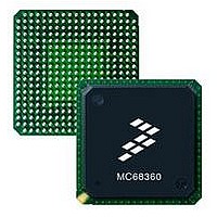
MC68EN360CAI25L Freescale Semiconductor, MC68EN360CAI25L Datasheet - Page 417

MC68EN360CAI25L
Manufacturer Part Number
MC68EN360CAI25L
Description
IC MPU QUICC 25MHZ 240-FQFP
Manufacturer
Freescale Semiconductor
Series
MC68000r
Datasheets
1.MC68EN302AG20BT.pdf
(8 pages)
2.MC68EN360VR25L.pdf
(14 pages)
3.MC68EN360VR25L.pdf
(2 pages)
4.MC68EN360CAI25L.pdf
(962 pages)
Specifications of MC68EN360CAI25L
Processor Type
M683xx 32-Bit
Speed
25MHz
Voltage
5V
Mounting Type
Surface Mount
Package / Case
240-FQFP
Core Size
32 Bit
Cpu Speed
25MHz
Embedded Interface Type
SCP, TDM
Digital Ic Case Style
FQFP
No. Of Pins
240
Supply Voltage Range
4.75V To 5.25V
Rohs Compliant
Yes
Family Name
M68xxx
Device Core
ColdFire
Device Core Size
32b
Frequency (max)
25MHz
Instruction Set Architecture
RISC
Supply Voltage 1 (typ)
5V
Operating Supply Voltage (max)
5.25V
Operating Supply Voltage (min)
4.75V
Operating Temp Range
-40C to 85C
Operating Temperature Classification
Industrial
Mounting
Surface Mount
Pin Count
240
Package Type
FQFP
Lead Free Status / RoHS Status
Lead free / RoHS Compliant
Features
-
Lead Free Status / Rohs Status
Compliant
Available stocks
Company
Part Number
Manufacturer
Quantity
Price
Company:
Part Number:
MC68EN360CAI25L
Manufacturer:
APLHA
Quantity:
12 000
Company:
Part Number:
MC68EN360CAI25L
Manufacturer:
Freescale Semiconductor
Quantity:
10 000
Part Number:
MC68EN360CAI25L
Manufacturer:
FREESCALE
Quantity:
20 000
- MC68EN302AG20BT PDF datasheet
- MC68EN360VR25L PDF datasheet #2
- MC68EN360VR25L PDF datasheet #3
- MC68EN360CAI25L PDF datasheet #4
- Current page: 417 of 962
- Download datasheet (4Mb)
The QUICC can identify and support each IDL channel or can output strobe lines for inter-
facing devices that do not support the IDL bus.
The IDL signals for each transmit and receive channel are as follows:
The basic rate IDL bus has three channels:
There are two definitions of the IDL bus frame structure: 8 bits and 10 bits (see Figure 7-33).
The difference between them is only the channel order within the frame.
The QUICC supports all channels of the IDL bus in the basic rate. Each bit in the IDL frame
can be routed to every SCC and SMC or can assert a strobe output for supporting an exter-
nal device.
1. L1RCLKx—IDL clock; input to the QUICC.
2. L1RSYNCx—IDL sync signal; input to the QUICC. This signal indicates that the clock
3. L1RXDx—IDL receive data; input to the QUICC. Valid only for the bits that are
4. L1TXDx—IDL transmit data; output from the QUICC. Valid only for the bits that are
5. L1RQx—IDL request permission to transmit on the D channel; output from the QUICC
6. L1GRx—IDL grant permission to transmit on the D Channel; input to the QUICC on
• B1—64 kbps bearer channel
• B2—64 kbps bearer channel
• D—16 kbps signaling channel
periods following the pulse designate the IDL frame.
supported by the IDL; ignored for other signals that may be present.
supported by the IDL; three-stated otherwise.
on L1RQx pin.
L1TSYNCx pin.
x = a and b for TDMa and TDMb.
Previous versions of Motorola’s IDL-defined bit functions, called
auxiliary (A) and maintenance (M), were eliminated from the IDL
definition when it was decided that the IDL control channel would
be out-of-band. They were defined as a subset of the Motorola
SPI format called serial control port (SCP). If a user wishes to
implement the A and M bit functions as originally defined, the
TSA may be programmed to access these bits and to route them
transparently to an SCC or SMC. To perform the out-of-band
signaling required, the QUICC’s SPI may be used.
Freescale Semiconductor, Inc.
For More Information On This Product,
MC68360 USER’S MANUAL
Go to: www.freescale.com
NOTE
NOTE
Serial Interface with Time Slot Assigner
Related parts for MC68EN360CAI25L
Image
Part Number
Description
Manufacturer
Datasheet
Request
R
Part Number:
Description:
Manufacturer:
Freescale Semiconductor, Inc
Datasheet:
Part Number:
Description:
Manufacturer:
Freescale Semiconductor, Inc
Datasheet:
Part Number:
Description:
Manufacturer:
Freescale Semiconductor, Inc
Datasheet:
Part Number:
Description:
Manufacturer:
Freescale Semiconductor, Inc
Datasheet:
Part Number:
Description:
Manufacturer:
Freescale Semiconductor, Inc
Datasheet:
Part Number:
Description:
Manufacturer:
Freescale Semiconductor, Inc
Datasheet:
Part Number:
Description:
Manufacturer:
Freescale Semiconductor, Inc
Datasheet:
Part Number:
Description:
Manufacturer:
Freescale Semiconductor, Inc
Datasheet:
Part Number:
Description:
Manufacturer:
Freescale Semiconductor, Inc
Datasheet:
Part Number:
Description:
Manufacturer:
Freescale Semiconductor, Inc
Datasheet:
Part Number:
Description:
Manufacturer:
Freescale Semiconductor, Inc
Datasheet:
Part Number:
Description:
Manufacturer:
Freescale Semiconductor, Inc
Datasheet:
Part Number:
Description:
Manufacturer:
Freescale Semiconductor, Inc
Datasheet:
Part Number:
Description:
Manufacturer:
Freescale Semiconductor, Inc
Datasheet:
Part Number:
Description:
Manufacturer:
Freescale Semiconductor, Inc
Datasheet:


