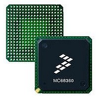
MC68EN360CAI25L Freescale Semiconductor, MC68EN360CAI25L Datasheet - Page 305

MC68EN360CAI25L
Manufacturer Part Number
MC68EN360CAI25L
Description
IC MPU QUICC 25MHZ 240-FQFP
Manufacturer
Freescale Semiconductor
Series
MC68000r
Datasheets
1.MC68EN302AG20BT.pdf
(8 pages)
2.MC68EN360VR25L.pdf
(14 pages)
3.MC68EN360VR25L.pdf
(2 pages)
4.MC68EN360CAI25L.pdf
(962 pages)
Specifications of MC68EN360CAI25L
Processor Type
M683xx 32-Bit
Speed
25MHz
Voltage
5V
Mounting Type
Surface Mount
Package / Case
240-FQFP
Core Size
32 Bit
Cpu Speed
25MHz
Embedded Interface Type
SCP, TDM
Digital Ic Case Style
FQFP
No. Of Pins
240
Supply Voltage Range
4.75V To 5.25V
Rohs Compliant
Yes
Family Name
M68xxx
Device Core
ColdFire
Device Core Size
32b
Frequency (max)
25MHz
Instruction Set Architecture
RISC
Supply Voltage 1 (typ)
5V
Operating Supply Voltage (max)
5.25V
Operating Supply Voltage (min)
4.75V
Operating Temp Range
-40C to 85C
Operating Temperature Classification
Industrial
Mounting
Surface Mount
Pin Count
240
Package Type
FQFP
Lead Free Status / RoHS Status
Lead free / RoHS Compliant
Features
-
Lead Free Status / Rohs Status
Compliant
Available stocks
Company
Part Number
Manufacturer
Quantity
Price
Company:
Part Number:
MC68EN360CAI25L
Manufacturer:
APLHA
Quantity:
12 000
Company:
Part Number:
MC68EN360CAI25L
Manufacturer:
Freescale Semiconductor
Quantity:
10 000
Part Number:
MC68EN360CAI25L
Manufacturer:
FREESCALE
Quantity:
20 000
- MC68EN302AG20BT PDF datasheet
- MC68EN360VR25L PDF datasheet #2
- MC68EN360VR25L PDF datasheet #3
- MC68EN360CAI25L PDF datasheet #4
- Current page: 305 of 962
- Download datasheet (4Mb)
the RAS signal of the DRAM bank. This RAS signal will remain active until another DRAM
bank is accessed. The page size is determined by the PGS bits in the GMR.
If a different bank of DRAM is accessed, followed by an access to a DRAM bank on which
page mode is selected, then the DRAM controller negates the RAS signal to the other bank
and asserts the particular RAS line for the page mode bank, followed by the rest of the
DRAM access. This is called a page mode normal cycle.
On each access to a DRAM bank in which the page mode is enabled and the previous
DRAM cycle was to that bank, the address of the last access to this bank is compared to the
current address. If the two addresses fall within the same page, then the access cycle
begins immediately with the assertion of the column address and CAS signal. This is called
a page hit.
In case of a page miss (the address of the last access and current address do not fall within
the same page), the RAS signal must be negated and held high for a period that matches
the value programmed in the WBTQ control field of the current DRAM region, and then a full
cycle (including row and column phases) is executed. This is the slowest DRAM access
since the RAS signal must first be negated, followed by the precharge time.
Since it is difficult to predict the performance impact of page mode, the user may wish to try
the application software with and without page mode enabled, and compare the results. The
ability to concentrate the code/data accesses into the same page of the DRAM is central to
achieving a performance improvement.
Some systems will need an additional wait state to perform write cycles during a page hit.
To gain a wait state, set the delay write cycle for the QUICC DWQ bit in the GMR of the
DRAM bank.
6.12.3 DRAM Burst Access Support
The DRAM controller supports burst accesses made by an external MC68EC040 (or other
MC68040 family member) if the BACK40 bit is set in the BR. The MC68EC040 requests a
burst to be performed with a line-fill indication on the SIZx pins (SIZ = 11) and the TTx pins.
In this case, the DRAM controller performs a normal access (RAS and CAS), followed by
requests to the DRAM for the next three sequential long-word operands (CAS only). The
DRAM controller automatically increments the addresses to the DRAM using the BADDR3–
BADDR2 pins.
The length of an MC68EC040 burst cycle can be distinguished from the length of the initial
access with the BCYC bits of the OR.
Page mode is supported only for the internal QUICC cycles or
external MC68030/QUICC cycles.
If any two DRAM banks overlap each other in their address
space, page mode must not be selected for either of those
banks.
Freescale Semiconductor, Inc.
For More Information On This Product,
MC68360 USER’S MANUAL
Go to: www.freescale.com
NOTES
System Integration Module (SIM60)
Related parts for MC68EN360CAI25L
Image
Part Number
Description
Manufacturer
Datasheet
Request
R
Part Number:
Description:
Manufacturer:
Freescale Semiconductor, Inc
Datasheet:
Part Number:
Description:
Manufacturer:
Freescale Semiconductor, Inc
Datasheet:
Part Number:
Description:
Manufacturer:
Freescale Semiconductor, Inc
Datasheet:
Part Number:
Description:
Manufacturer:
Freescale Semiconductor, Inc
Datasheet:
Part Number:
Description:
Manufacturer:
Freescale Semiconductor, Inc
Datasheet:
Part Number:
Description:
Manufacturer:
Freescale Semiconductor, Inc
Datasheet:
Part Number:
Description:
Manufacturer:
Freescale Semiconductor, Inc
Datasheet:
Part Number:
Description:
Manufacturer:
Freescale Semiconductor, Inc
Datasheet:
Part Number:
Description:
Manufacturer:
Freescale Semiconductor, Inc
Datasheet:
Part Number:
Description:
Manufacturer:
Freescale Semiconductor, Inc
Datasheet:
Part Number:
Description:
Manufacturer:
Freescale Semiconductor, Inc
Datasheet:
Part Number:
Description:
Manufacturer:
Freescale Semiconductor, Inc
Datasheet:
Part Number:
Description:
Manufacturer:
Freescale Semiconductor, Inc
Datasheet:
Part Number:
Description:
Manufacturer:
Freescale Semiconductor, Inc
Datasheet:
Part Number:
Description:
Manufacturer:
Freescale Semiconductor, Inc
Datasheet:


