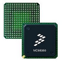
MC68EN360CAI25L Freescale Semiconductor, MC68EN360CAI25L Datasheet - Page 648

MC68EN360CAI25L
Manufacturer Part Number
MC68EN360CAI25L
Description
IC MPU QUICC 25MHZ 240-FQFP
Manufacturer
Freescale Semiconductor
Series
MC68000r
Datasheets
1.MC68EN302AG20BT.pdf
(8 pages)
2.MC68EN360VR25L.pdf
(14 pages)
3.MC68EN360VR25L.pdf
(2 pages)
4.MC68EN360CAI25L.pdf
(962 pages)
Specifications of MC68EN360CAI25L
Processor Type
M683xx 32-Bit
Speed
25MHz
Voltage
5V
Mounting Type
Surface Mount
Package / Case
240-FQFP
Core Size
32 Bit
Cpu Speed
25MHz
Embedded Interface Type
SCP, TDM
Digital Ic Case Style
FQFP
No. Of Pins
240
Supply Voltage Range
4.75V To 5.25V
Rohs Compliant
Yes
Family Name
M68xxx
Device Core
ColdFire
Device Core Size
32b
Frequency (max)
25MHz
Instruction Set Architecture
RISC
Supply Voltage 1 (typ)
5V
Operating Supply Voltage (max)
5.25V
Operating Supply Voltage (min)
4.75V
Operating Temp Range
-40C to 85C
Operating Temperature Classification
Industrial
Mounting
Surface Mount
Pin Count
240
Package Type
FQFP
Lead Free Status / RoHS Status
Lead free / RoHS Compliant
Features
-
Lead Free Status / Rohs Status
Compliant
Available stocks
Company
Part Number
Manufacturer
Quantity
Price
Company:
Part Number:
MC68EN360CAI25L
Manufacturer:
APLHA
Quantity:
12 000
Company:
Part Number:
MC68EN360CAI25L
Manufacturer:
Freescale Semiconductor
Quantity:
10 000
Part Number:
MC68EN360CAI25L
Manufacturer:
FREESCALE
Quantity:
20 000
- MC68EN302AG20BT PDF datasheet
- MC68EN360VR25L PDF datasheet #2
- MC68EN360VR25L PDF datasheet #3
- MC68EN360CAI25L PDF datasheet #4
- Current page: 648 of 962
- Download datasheet (4Mb)
Serial Peripheral Interface (SPI)
7.12.5.4.3 INIT RX PARAMETERS Command. This command initializes all the receive
parameters in this serial channel’s parameter RAM to their reset state. This command
should only be issued when the receiver is disabled. Note that the INIT TX AND RX PARAM-
ETERS command may also be used to reset both receive and transmit parameters.
7.12.5.5 SPI BUFFER DESCRIPTOR RING. The data associated with the SPI is stored in
buffers, which are referenced by BDs organized in a BD ring located in the dual-port RAM
(see Figure 7-83). This ring has the same basic configuration as those used by the SCCs
and SMCs.
The BD ring allows the user to define buffers for transmission and buffers for reception. Each
BD ring forms a circular queue. The CP confirms reception and transmission or indicates
error conditions using the BDs to inform the processor that the buffers have been serviced.
The actual buffers may reside in either external memory or internal memory. Data buffers
may reside in the parameter area of an SCC if it is not enabled.
7.12.5.5.1 SPI Receive Buffer Descriptor (Rx BD). The CP reports information about
each buffer of received data using Rx BDs. The CP closes the current buffer, generates a
maskable interrupt, and starts receiving data in the next buffer when the current buffer is full.
Additionally, it will close the buffer when the SPI is configured as a slave and the SPISEL
pin goes to an inactive state, indicating that the reception process is terminated.
The first word of the Rx BD contains status and control bits. These bits are prepared by the
user before reception and are set by the CP after the buffer has been closed. The second
word contains the data length, in bytes, that was received. The third and fourth words con-
tain a pointer that always points to the beginning of the received data buffer.
7-324
POINTER TO SPI
POINTER TO SPI
DUAL-PORT RAM
TX DATA BUFFER
TX RING
RX RING
Freescale Semiconductor, Inc.
Figure 7-83. SPI Memory Structure
For More Information On This Product,
MC68360 USER’S MANUAL
Go to: www.freescale.com
FRAME STATUS
FRAME STATUS
DATA POINTER
DATA POINTER
DATA LENGTH
DATA LENGTH
TX BD RING
RX BD RING
EXTERNAL MEMORY
TX DATA BUFFER
RX DATA BUFFER
Related parts for MC68EN360CAI25L
Image
Part Number
Description
Manufacturer
Datasheet
Request
R
Part Number:
Description:
Manufacturer:
Freescale Semiconductor, Inc
Datasheet:
Part Number:
Description:
Manufacturer:
Freescale Semiconductor, Inc
Datasheet:
Part Number:
Description:
Manufacturer:
Freescale Semiconductor, Inc
Datasheet:
Part Number:
Description:
Manufacturer:
Freescale Semiconductor, Inc
Datasheet:
Part Number:
Description:
Manufacturer:
Freescale Semiconductor, Inc
Datasheet:
Part Number:
Description:
Manufacturer:
Freescale Semiconductor, Inc
Datasheet:
Part Number:
Description:
Manufacturer:
Freescale Semiconductor, Inc
Datasheet:
Part Number:
Description:
Manufacturer:
Freescale Semiconductor, Inc
Datasheet:
Part Number:
Description:
Manufacturer:
Freescale Semiconductor, Inc
Datasheet:
Part Number:
Description:
Manufacturer:
Freescale Semiconductor, Inc
Datasheet:
Part Number:
Description:
Manufacturer:
Freescale Semiconductor, Inc
Datasheet:
Part Number:
Description:
Manufacturer:
Freescale Semiconductor, Inc
Datasheet:
Part Number:
Description:
Manufacturer:
Freescale Semiconductor, Inc
Datasheet:
Part Number:
Description:
Manufacturer:
Freescale Semiconductor, Inc
Datasheet:
Part Number:
Description:
Manufacturer:
Freescale Semiconductor, Inc
Datasheet:


