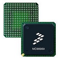
MC68EN360CAI25L Freescale Semiconductor, MC68EN360CAI25L Datasheet - Page 313

MC68EN360CAI25L
Manufacturer Part Number
MC68EN360CAI25L
Description
IC MPU QUICC 25MHZ 240-FQFP
Manufacturer
Freescale Semiconductor
Series
MC68000r
Datasheets
1.MC68EN302AG20BT.pdf
(8 pages)
2.MC68EN360VR25L.pdf
(14 pages)
3.MC68EN360VR25L.pdf
(2 pages)
4.MC68EN360CAI25L.pdf
(962 pages)
Specifications of MC68EN360CAI25L
Processor Type
M683xx 32-Bit
Speed
25MHz
Voltage
5V
Mounting Type
Surface Mount
Package / Case
240-FQFP
Core Size
32 Bit
Cpu Speed
25MHz
Embedded Interface Type
SCP, TDM
Digital Ic Case Style
FQFP
No. Of Pins
240
Supply Voltage Range
4.75V To 5.25V
Rohs Compliant
Yes
Family Name
M68xxx
Device Core
ColdFire
Device Core Size
32b
Frequency (max)
25MHz
Instruction Set Architecture
RISC
Supply Voltage 1 (typ)
5V
Operating Supply Voltage (max)
5.25V
Operating Supply Voltage (min)
4.75V
Operating Temp Range
-40C to 85C
Operating Temperature Classification
Industrial
Mounting
Surface Mount
Pin Count
240
Package Type
FQFP
Lead Free Status / RoHS Status
Lead free / RoHS Compliant
Features
-
Lead Free Status / Rohs Status
Compliant
Available stocks
Company
Part Number
Manufacturer
Quantity
Price
Company:
Part Number:
MC68EN360CAI25L
Manufacturer:
APLHA
Quantity:
12 000
Company:
Part Number:
MC68EN360CAI25L
Manufacturer:
Freescale Semiconductor
Quantity:
10 000
Part Number:
MC68EN360CAI25L
Manufacturer:
FREESCALE
Quantity:
20 000
- MC68EN302AG20BT PDF datasheet
- MC68EN360VR25L PDF datasheet #2
- MC68EN360VR25L PDF datasheet #3
- MC68EN360CAI25L PDF datasheet #4
- Current page: 313 of 962
- Download datasheet (4Mb)
NCS—No CPU Space
GAMX—Global Address Mux Enable
Bits 4–0—Reserved
6.13.2 Memory Controller Status Register (MSTAT)
The MSTAT register reports memory controller error information to the user. These bits are
set, regardless of whether an internal or external master originated the cycle. Bits are reset
by writing a one to that bit; writing a zero has no effect. The register may be read at any time
and is cleared by reset. No interrupts are generated from this register; however, an internal
controller may sample TS with a one-clock-phase delay. This will delay the assertion of
the CS or RAS in the MC68EC040 memory cycle by one clock phase. It will delay the rest
of the bus cycle by one clock (effectively adding one extra clock cycle per bus cycle).
This attribute specifies whether the CS/RAS signal will assert on a CPU space access cy-
cle. If both supervisor data and program accesses are desired, while ignoring CPU space
accesses, then this bit should be set. (Note that an interrupt acknowledge cycle is a CPU
space access, but a user or supervisor read/write cycle is not.) A CPU space access has
the function code value 0111.
This attribute determines whether the QUICC will provide internal address multiplexing for
DRAM banks. If not, the address multiplexing must be provided externally, with the
QUICC’s AMUX pin being used to control the multiplexers. AMUX is high to signify the
row, low to signify the column address, and then negated (high) at the end of the DRAM
bus cycle.
There are two situations in which the user may wish to provide address multiplexing ex-
ternally. First, external multiplexers are required when an external master exists in the
system and that external master needs to access the DRAM. Second, using external ad-
dress multiplexing causes the clock to address valid timing as slightly accelerated, which
may be beneficial in certain high-performance situations.
0 = Do not sample TS.
1 = Sample TS prior to using it.
0 = Assert CS/RAS on CPU space accesses (default).
1 = Suppress CS/RAS on CPU space accesses.
0 = Disable internal address multiplexing for all DRAM banks.
1 = Enable internal address multiplexing for all DRAM banks.
In general, the user determines whether this bit must be set be-
fore to selecting the WBT40 and TCYC bits.
In default state, user should program the FC3-FC0 in both the
Option Registers and Base Registers so that CS/RAS will not
get asserted in an undesirable address range.
Freescale Semiconductor, Inc.
For More Information On This Product,
MC68360 USER’S MANUAL
Go to: www.freescale.com
NOTE
NOTE
System Integration Module (SIM60)
Related parts for MC68EN360CAI25L
Image
Part Number
Description
Manufacturer
Datasheet
Request
R
Part Number:
Description:
Manufacturer:
Freescale Semiconductor, Inc
Datasheet:
Part Number:
Description:
Manufacturer:
Freescale Semiconductor, Inc
Datasheet:
Part Number:
Description:
Manufacturer:
Freescale Semiconductor, Inc
Datasheet:
Part Number:
Description:
Manufacturer:
Freescale Semiconductor, Inc
Datasheet:
Part Number:
Description:
Manufacturer:
Freescale Semiconductor, Inc
Datasheet:
Part Number:
Description:
Manufacturer:
Freescale Semiconductor, Inc
Datasheet:
Part Number:
Description:
Manufacturer:
Freescale Semiconductor, Inc
Datasheet:
Part Number:
Description:
Manufacturer:
Freescale Semiconductor, Inc
Datasheet:
Part Number:
Description:
Manufacturer:
Freescale Semiconductor, Inc
Datasheet:
Part Number:
Description:
Manufacturer:
Freescale Semiconductor, Inc
Datasheet:
Part Number:
Description:
Manufacturer:
Freescale Semiconductor, Inc
Datasheet:
Part Number:
Description:
Manufacturer:
Freescale Semiconductor, Inc
Datasheet:
Part Number:
Description:
Manufacturer:
Freescale Semiconductor, Inc
Datasheet:
Part Number:
Description:
Manufacturer:
Freescale Semiconductor, Inc
Datasheet:
Part Number:
Description:
Manufacturer:
Freescale Semiconductor, Inc
Datasheet:


