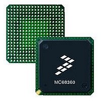
MC68EN360CAI25L Freescale Semiconductor, MC68EN360CAI25L Datasheet - Page 427

MC68EN360CAI25L
Manufacturer Part Number
MC68EN360CAI25L
Description
IC MPU QUICC 25MHZ 240-FQFP
Manufacturer
Freescale Semiconductor
Series
MC68000r
Datasheets
1.MC68EN302AG20BT.pdf
(8 pages)
2.MC68EN360VR25L.pdf
(14 pages)
3.MC68EN360VR25L.pdf
(2 pages)
4.MC68EN360CAI25L.pdf
(962 pages)
Specifications of MC68EN360CAI25L
Processor Type
M683xx 32-Bit
Speed
25MHz
Voltage
5V
Mounting Type
Surface Mount
Package / Case
240-FQFP
Core Size
32 Bit
Cpu Speed
25MHz
Embedded Interface Type
SCP, TDM
Digital Ic Case Style
FQFP
No. Of Pins
240
Supply Voltage Range
4.75V To 5.25V
Rohs Compliant
Yes
Family Name
M68xxx
Device Core
ColdFire
Device Core Size
32b
Frequency (max)
25MHz
Instruction Set Architecture
RISC
Supply Voltage 1 (typ)
5V
Operating Supply Voltage (max)
5.25V
Operating Supply Voltage (min)
4.75V
Operating Temp Range
-40C to 85C
Operating Temperature Classification
Industrial
Mounting
Surface Mount
Pin Count
240
Package Type
FQFP
Lead Free Status / RoHS Status
Lead free / RoHS Compliant
Features
-
Lead Free Status / Rohs Status
Compliant
Available stocks
Company
Part Number
Manufacturer
Quantity
Price
Company:
Part Number:
MC68EN360CAI25L
Manufacturer:
APLHA
Quantity:
12 000
Company:
Part Number:
MC68EN360CAI25L
Manufacturer:
Freescale Semiconductor
Quantity:
10 000
Part Number:
MC68EN360CAI25L
Manufacturer:
FREESCALE
Quantity:
20 000
- MC68EN302AG20BT PDF datasheet
- MC68EN360VR25L PDF datasheet #2
- MC68EN360VR25L PDF datasheet #3
- MC68EN360CAI25L PDF datasheet #4
- Current page: 427 of 962
- Download datasheet (4Mb)
The SCC4 in NMSI mode has its own set of modem control pins:
The SMC1 in NMSI mode has its own set of modem control pins:
The SMC2 in NMSI mode has its own set of modem control pins:
Any SCC or SMC that requires fewer pins that those listed may use that pin for another func-
tion or configure that pin as a parallel I/O pin.
Since some SCCs use external clock pins CLK1–CLK4 and other SCCs use external clock
pins CLK5–CLK8, it might seem that there is no way to provide one external clock source
on one CLK pin to be used by all four SCCs. However, the QUICC provides a simple clock
bridge function from external CLK8 to the internal CLK4 connection, even if the CLK4 pin is
used for another of its programmable functions. This configuration allows SCC1/SCC2 to
share clocks with SCC3/SCC4 without wasting an external pin. This is shown in the port A
registers in 7.14.4 Port A Registers.
7.9 BAUD RATE GENERATORS (BRGS)
The CPM contains four, independent, identical BRGs that can be used with the SCCs and
SMCs. The clocks produced in the BRG are sent to the bank-of-clocks selection logic, where
they can be routed to the SCCs and/or SMCs. The bank-of-clocks logic is described in 7.8.9
NMSI Configuration. In addition, the output of the BRG may be routed to a pin to be used
externally. The main features of the BRGs are as follows:
• Four, Independent, Identical BRGs
• On-the-Fly Changes Allowed
• Each BRG May Be Routed to One or More SCCs or SMCs
• A 16 Divider Option Allows Slow Baud Rates at High System Frequencies
• Each BRG Contains an Autobaud Support Option
TXD4
RXD4
TCLK4 <- BRG1–BRG4, CLK5–CLK8
RCLK4 <- BRG1–BRG4, CLK5–CLK8
RTS4
CTS4
CD4
SMTXD1
SMRXD1
SMCLK1 <- BRG1–BRG4, CLK1–CLK4
SMSYN1 (used only in the totally transparent protocol)
SMTXD2
SMRXD2
SMCLK2 <- BRG1–BRG4, CLK5–CLK8
SMSYN2 (used only in the totally transparent protocol)
Freescale Semiconductor, Inc.
For More Information On This Product,
MC68360 USER’S MANUAL
Go to: www.freescale.com
Baud Rate Generators (BRGs)
Related parts for MC68EN360CAI25L
Image
Part Number
Description
Manufacturer
Datasheet
Request
R
Part Number:
Description:
Manufacturer:
Freescale Semiconductor, Inc
Datasheet:
Part Number:
Description:
Manufacturer:
Freescale Semiconductor, Inc
Datasheet:
Part Number:
Description:
Manufacturer:
Freescale Semiconductor, Inc
Datasheet:
Part Number:
Description:
Manufacturer:
Freescale Semiconductor, Inc
Datasheet:
Part Number:
Description:
Manufacturer:
Freescale Semiconductor, Inc
Datasheet:
Part Number:
Description:
Manufacturer:
Freescale Semiconductor, Inc
Datasheet:
Part Number:
Description:
Manufacturer:
Freescale Semiconductor, Inc
Datasheet:
Part Number:
Description:
Manufacturer:
Freescale Semiconductor, Inc
Datasheet:
Part Number:
Description:
Manufacturer:
Freescale Semiconductor, Inc
Datasheet:
Part Number:
Description:
Manufacturer:
Freescale Semiconductor, Inc
Datasheet:
Part Number:
Description:
Manufacturer:
Freescale Semiconductor, Inc
Datasheet:
Part Number:
Description:
Manufacturer:
Freescale Semiconductor, Inc
Datasheet:
Part Number:
Description:
Manufacturer:
Freescale Semiconductor, Inc
Datasheet:
Part Number:
Description:
Manufacturer:
Freescale Semiconductor, Inc
Datasheet:
Part Number:
Description:
Manufacturer:
Freescale Semiconductor, Inc
Datasheet:


