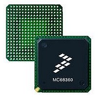
MC68EN360CAI25L Freescale Semiconductor, MC68EN360CAI25L Datasheet - Page 79

MC68EN360CAI25L
Manufacturer Part Number
MC68EN360CAI25L
Description
IC MPU QUICC 25MHZ 240-FQFP
Manufacturer
Freescale Semiconductor
Series
MC68000r
Datasheets
1.MC68EN302AG20BT.pdf
(8 pages)
2.MC68EN360VR25L.pdf
(14 pages)
3.MC68EN360VR25L.pdf
(2 pages)
4.MC68EN360CAI25L.pdf
(962 pages)
Specifications of MC68EN360CAI25L
Processor Type
M683xx 32-Bit
Speed
25MHz
Voltage
5V
Mounting Type
Surface Mount
Package / Case
240-FQFP
Core Size
32 Bit
Cpu Speed
25MHz
Embedded Interface Type
SCP, TDM
Digital Ic Case Style
FQFP
No. Of Pins
240
Supply Voltage Range
4.75V To 5.25V
Rohs Compliant
Yes
Family Name
M68xxx
Device Core
ColdFire
Device Core Size
32b
Frequency (max)
25MHz
Instruction Set Architecture
RISC
Supply Voltage 1 (typ)
5V
Operating Supply Voltage (max)
5.25V
Operating Supply Voltage (min)
4.75V
Operating Temp Range
-40C to 85C
Operating Temperature Classification
Industrial
Mounting
Surface Mount
Pin Count
240
Package Type
FQFP
Lead Free Status / RoHS Status
Lead free / RoHS Compliant
Features
-
Lead Free Status / Rohs Status
Compliant
Available stocks
Company
Part Number
Manufacturer
Quantity
Price
Company:
Part Number:
MC68EN360CAI25L
Manufacturer:
APLHA
Quantity:
12 000
Company:
Part Number:
MC68EN360CAI25L
Manufacturer:
Freescale Semiconductor
Quantity:
10 000
Part Number:
MC68EN360CAI25L
Manufacturer:
FREESCALE
Quantity:
20 000
- MC68EN302AG20BT PDF datasheet
- MC68EN360VR25L PDF datasheet #2
- MC68EN360VR25L PDF datasheet #3
- MC68EN360CAI25L PDF datasheet #4
- Current page: 79 of 962
- Download datasheet (4Mb)
4.1.1 Bus Control Signals
The QUICC initiates a bus cycle by driving the address, size, function code, and read/write
outputs. At the beginning of a bus cycle, SIZ1 and SIZ0 are driven with the FC signals. SIZ1
and SIZ0 indicate the number of bytes remaining to be transferred during an operand cycle
(consisting of one or more bus cycles). Table 4-3 lists the encoding of SIZ1 and SIZ0. These
signals are valid while AS is asserted.
The R/W signal determines the direction of the transfer during a bus cycle. Driven at the
beginning of a bus cycle, R/W is valid while AS is asserted. R/W only transitions when a write
cycle is preceded by a read cycle or vice versa. The signal may remain low for consecutive
write cycles.
The RMC signal is asserted at the beginning of the first bus cycle of a read-modify-write
operation and remains asserted until completion of the final bus cycle of the operation.
4.1.2 Function Codes (FC3–FC0)
The FCx signals are outputs that indicate one of 16 address spaces to which the address
applies. Fifteen of these spaces are designated as either a normal or DMA cycle, user or
supervisor, and program or data spaces. One other address space is designated as CPU
space to allow the CPU32+ to acquire specific control information not normally associated
with read or write bus cycles. The FCx signals are valid while AS is asserted.
Function codes (see Table 4-1) can be considered as extensions of the 32-bit address that
can provide up to eight different 4-Gbyte address spaces. Function codes are automatically
generated by the CPU32+ to select address spaces for data and program at both user and
supervisor privilege levels, and a CPU address space for processor functions. User pro-
grams access only their own program and data areas to increase protection of system integ-
rity and can be restricted from accessing other information. The S-bit in the CPU32+ status
register is set for supervisor accesses and cleared for user accesses to provide differentia-
tion. Refer to 4.4 CPU Space Cycles for more information.
3
0
0
0
0
0
0
0
0
1
Freescale Semiconductor, Inc.
Function Code Bits
For More Information On This Product,
Table 4-1. Address Space Encoding
2
0
0
0
0
1
1
1
1
x
MC68360 USER’S MANUAL
Go to: www.freescale.com
1
0
0
1
1
0
0
1
1
x
0
0
1
0
1
0
1
0
1
x
Reserved (Motorola)
User Data Space
User Program Space
Reserved (User)
Reserved (Motorola)
Supervisor Data Space
Supervisor Program Space
Supervisor CPU Space
DMA space
Address Spaces
Bus Operation
Related parts for MC68EN360CAI25L
Image
Part Number
Description
Manufacturer
Datasheet
Request
R
Part Number:
Description:
Manufacturer:
Freescale Semiconductor, Inc
Datasheet:
Part Number:
Description:
Manufacturer:
Freescale Semiconductor, Inc
Datasheet:
Part Number:
Description:
Manufacturer:
Freescale Semiconductor, Inc
Datasheet:
Part Number:
Description:
Manufacturer:
Freescale Semiconductor, Inc
Datasheet:
Part Number:
Description:
Manufacturer:
Freescale Semiconductor, Inc
Datasheet:
Part Number:
Description:
Manufacturer:
Freescale Semiconductor, Inc
Datasheet:
Part Number:
Description:
Manufacturer:
Freescale Semiconductor, Inc
Datasheet:
Part Number:
Description:
Manufacturer:
Freescale Semiconductor, Inc
Datasheet:
Part Number:
Description:
Manufacturer:
Freescale Semiconductor, Inc
Datasheet:
Part Number:
Description:
Manufacturer:
Freescale Semiconductor, Inc
Datasheet:
Part Number:
Description:
Manufacturer:
Freescale Semiconductor, Inc
Datasheet:
Part Number:
Description:
Manufacturer:
Freescale Semiconductor, Inc
Datasheet:
Part Number:
Description:
Manufacturer:
Freescale Semiconductor, Inc
Datasheet:
Part Number:
Description:
Manufacturer:
Freescale Semiconductor, Inc
Datasheet:
Part Number:
Description:
Manufacturer:
Freescale Semiconductor, Inc
Datasheet:


