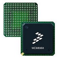
MC68EN360CAI25L Freescale Semiconductor, MC68EN360CAI25L Datasheet - Page 692

MC68EN360CAI25L
Manufacturer Part Number
MC68EN360CAI25L
Description
IC MPU QUICC 25MHZ 240-FQFP
Manufacturer
Freescale Semiconductor
Series
MC68000r
Datasheets
1.MC68EN302AG20BT.pdf
(8 pages)
2.MC68EN360VR25L.pdf
(14 pages)
3.MC68EN360VR25L.pdf
(2 pages)
4.MC68EN360CAI25L.pdf
(962 pages)
Specifications of MC68EN360CAI25L
Processor Type
M683xx 32-Bit
Speed
25MHz
Voltage
5V
Mounting Type
Surface Mount
Package / Case
240-FQFP
Core Size
32 Bit
Cpu Speed
25MHz
Embedded Interface Type
SCP, TDM
Digital Ic Case Style
FQFP
No. Of Pins
240
Supply Voltage Range
4.75V To 5.25V
Rohs Compliant
Yes
Family Name
M68xxx
Device Core
ColdFire
Device Core Size
32b
Frequency (max)
25MHz
Instruction Set Architecture
RISC
Supply Voltage 1 (typ)
5V
Operating Supply Voltage (max)
5.25V
Operating Supply Voltage (min)
4.75V
Operating Temp Range
-40C to 85C
Operating Temperature Classification
Industrial
Mounting
Surface Mount
Pin Count
240
Package Type
FQFP
Lead Free Status / RoHS Status
Lead free / RoHS Compliant
Features
-
Lead Free Status / Rohs Status
Compliant
Available stocks
Company
Part Number
Manufacturer
Quantity
Price
Company:
Part Number:
MC68EN360CAI25L
Manufacturer:
APLHA
Quantity:
12 000
Company:
Part Number:
MC68EN360CAI25L
Manufacturer:
Freescale Semiconductor
Quantity:
10 000
Part Number:
MC68EN360CAI25L
Manufacturer:
FREESCALE
Quantity:
20 000
- MC68EN302AG20BT PDF datasheet
- MC68EN360VR25L PDF datasheet #2
- MC68EN360VR25L PDF datasheet #3
- MC68EN360CAI25L PDF datasheet #4
- Current page: 692 of 962
- Download datasheet (4Mb)
Parallel I/O Ports
7.14.10.1 PORT C DATA REGISTER (PCDAT). When read, PCDAT always reflects the
current status of each line.
7.14.10.2 PORT C DATA DIRECTION REGISTER (PCDIR). PCDIR is a 16-bit register that
is cleared at system reset.
7.14.10.3 PORT C PIN ASSIGNMENT REGISTER (PCPAR). PCPAR is a 16-bit register
that is cleared at system reset.
7.14.10.4 PORT C SPECIAL OPTIONS (PCSO). PCSO is a 16-bit read-write register.
Each defined bit in the PCSO corresponds to a port C line (PC11–PC4 and PC1–PC0). The
PCSO is cleared at reset.
Bits 15–12, 3–2—Reserved
CDx—Carrier Detect
CTSx—Clear-To-Send
7-368
15
15
15
15
These bits should be written with zeros.
0
0
0
0 = PCx is a general-purpose interrupt I/O pin. (The SCC’s internal CDx signal is al-
1 = PCx is connected to the corresponding SCC signal input in addition to being a gen-
0 = PCx is a general-purpose interrupt I/O pin. (The SCC’s internal CTSx signal is al-
1 = PCx is connected to the corresponding SCC signal input in addition to being a gen-
14
14
14
14
0
0
0
ways asserted.) If PCDIR configures this pin as an input, this pin can generate an
interrupt to the CPU32+ core, as controlled by the PCINT bits.
eral-purpose interrupt pin.
ways asserted.) If PCDIR configures this pin as an input, this pin can generate an
interrupt to the CPU32+ core, as controlled by the PCINT bits.
eral-purpose interrupt pin.
—
13
13
13
13
0
0
0
12
12
12
12
0
0
0
DR11
DD11
CD4
D11
11
11
11
11
Freescale Semiconductor, Inc.
For More Information On This Product,
DR10
DD10
CTS4
D10
10
10
10
10
MC68360 USER’S MANUAL
Go to: www.freescale.com
DR9
DD9
CD3
D9
9
9
9
9
CTS3
DR8
DD8
D8
8
8
8
8
DR7
DD7
CD2
D7
7
7
7
7
CTS2
DR6
DD6
D6
6
6
6
6
DR5
DD5
CD1
D5
5
5
5
5
CTS1
DR4
DD4
D4
4
4
4
4
DR3
DD3
D3
3
3
3
3
DR2
DD2
D2
2
2
2
2
—
DR1
DD1
D1
1
1
1
1
DR0
DD0
D0
0
0
0
0
Related parts for MC68EN360CAI25L
Image
Part Number
Description
Manufacturer
Datasheet
Request
R
Part Number:
Description:
Manufacturer:
Freescale Semiconductor, Inc
Datasheet:
Part Number:
Description:
Manufacturer:
Freescale Semiconductor, Inc
Datasheet:
Part Number:
Description:
Manufacturer:
Freescale Semiconductor, Inc
Datasheet:
Part Number:
Description:
Manufacturer:
Freescale Semiconductor, Inc
Datasheet:
Part Number:
Description:
Manufacturer:
Freescale Semiconductor, Inc
Datasheet:
Part Number:
Description:
Manufacturer:
Freescale Semiconductor, Inc
Datasheet:
Part Number:
Description:
Manufacturer:
Freescale Semiconductor, Inc
Datasheet:
Part Number:
Description:
Manufacturer:
Freescale Semiconductor, Inc
Datasheet:
Part Number:
Description:
Manufacturer:
Freescale Semiconductor, Inc
Datasheet:
Part Number:
Description:
Manufacturer:
Freescale Semiconductor, Inc
Datasheet:
Part Number:
Description:
Manufacturer:
Freescale Semiconductor, Inc
Datasheet:
Part Number:
Description:
Manufacturer:
Freescale Semiconductor, Inc
Datasheet:
Part Number:
Description:
Manufacturer:
Freescale Semiconductor, Inc
Datasheet:
Part Number:
Description:
Manufacturer:
Freescale Semiconductor, Inc
Datasheet:
Part Number:
Description:
Manufacturer:
Freescale Semiconductor, Inc
Datasheet:


