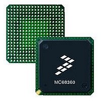
MC68EN360CAI25L Freescale Semiconductor, MC68EN360CAI25L Datasheet - Page 642

MC68EN360CAI25L
Manufacturer Part Number
MC68EN360CAI25L
Description
IC MPU QUICC 25MHZ 240-FQFP
Manufacturer
Freescale Semiconductor
Series
MC68000r
Datasheets
1.MC68EN302AG20BT.pdf
(8 pages)
2.MC68EN360VR25L.pdf
(14 pages)
3.MC68EN360VR25L.pdf
(2 pages)
4.MC68EN360CAI25L.pdf
(962 pages)
Specifications of MC68EN360CAI25L
Processor Type
M683xx 32-Bit
Speed
25MHz
Voltage
5V
Mounting Type
Surface Mount
Package / Case
240-FQFP
Core Size
32 Bit
Cpu Speed
25MHz
Embedded Interface Type
SCP, TDM
Digital Ic Case Style
FQFP
No. Of Pins
240
Supply Voltage Range
4.75V To 5.25V
Rohs Compliant
Yes
Family Name
M68xxx
Device Core
ColdFire
Device Core Size
32b
Frequency (max)
25MHz
Instruction Set Architecture
RISC
Supply Voltage 1 (typ)
5V
Operating Supply Voltage (max)
5.25V
Operating Supply Voltage (min)
4.75V
Operating Temp Range
-40C to 85C
Operating Temperature Classification
Industrial
Mounting
Surface Mount
Pin Count
240
Package Type
FQFP
Lead Free Status / RoHS Status
Lead free / RoHS Compliant
Features
-
Lead Free Status / Rohs Status
Compliant
Available stocks
Company
Part Number
Manufacturer
Quantity
Price
Company:
Part Number:
MC68EN360CAI25L
Manufacturer:
APLHA
Quantity:
12 000
Company:
Part Number:
MC68EN360CAI25L
Manufacturer:
Freescale Semiconductor
Quantity:
10 000
Part Number:
MC68EN360CAI25L
Manufacturer:
FREESCALE
Quantity:
20 000
- MC68EN302AG20BT PDF datasheet
- MC68EN360VR25L PDF datasheet #2
- MC68EN360VR25L PDF datasheet #3
- MC68EN360CAI25L PDF datasheet #4
- Current page: 642 of 962
- Download datasheet (4Mb)
Serial Peripheral Interface (SPI)
M/S—Master/Slave
EN—Enable SPI
LEN—Character Length
PM3–PM0—Prescale Modulus Select
SPI Examples with Different LEN Values
These examples use LEN to illustrate using the bits described above.To help map the pro-
cess, let g through v be binary symbols, x indicates a deleted bit, __ indicates original byte
boundaries, and _ indicates original nybble (4-bit) boundaries - both are used to aid read-
ability and to help understand the process. Once the data string image is determined, it is
always transmitted byte by byte with the lsb first.
Let the memory contain the following binary image:
7-318
The M/S bit configures the SPI to work as a master or a slave.
The EN bit enables the SPI operation. Note that SPIMOSI, SPIMISO, SPICLK, and
SPISEL should be configured to connect to the SPI as described in 7.14.7 Port B Regis-
ters. When the EN bit is cleared, the SPI is in a reset state and consumes minimal pow-
er—the SPI baud rate generator is not functioning and the input clock is disabled.
The LEN field specifies how many bits are in a character. The value 0000 corresponds to
1 bit, and the value 1111 corresponds to 16 bits. Acceptable values are in the range of 4
to 16 bits inclusive. Programming a value less than 4 bits may cause erratic behavior.
If the LEN value is less than or equal to a byte, there will be LEN number of valid bits in
every byte (8 bits) in memory. If the LEN value is greater than a byte, there will be LEN
number of valid bits in every word (16 bits) in memory (See the following example).
These four bits specify the divide ratio of the prescale divider in the SPI clock generator.
The BRGCLK is divided by 4 * ([PM3–PM0] + 1) giving a clock divide ratio of 4 to 64. The
clock has a 50% duty cycle.
0 = SPI is a slave.
1 = SPI is a master.
0 = SPI is disabled.
1 = SPI is enabled.
Example 1:
with LEN=4 (data size=5), the following data is selected:
with REV=0, the data string image is:
the order of the string appearing on the line, a byte at a time is:
with REV=1, the string has each byte reversed
the data string image is:
Other bits of the SPMODE should not be modified by the user
while EN is set.
msb
msb
msb
msb
Freescale Semiconductor, Inc.
For More Information On This Product,
nmlk_j__vuts_r
MC68360 USER’S MANUAL
Go to: www.freescale.com
nmlk_j__vuts_r
ghij_klmn __opqr_stuv
xxxj_klmn__xxxr_stuv
j_klmn__r_stuv
NOTE
lsb
lsb
lsb
lsb
Related parts for MC68EN360CAI25L
Image
Part Number
Description
Manufacturer
Datasheet
Request
R
Part Number:
Description:
Manufacturer:
Freescale Semiconductor, Inc
Datasheet:
Part Number:
Description:
Manufacturer:
Freescale Semiconductor, Inc
Datasheet:
Part Number:
Description:
Manufacturer:
Freescale Semiconductor, Inc
Datasheet:
Part Number:
Description:
Manufacturer:
Freescale Semiconductor, Inc
Datasheet:
Part Number:
Description:
Manufacturer:
Freescale Semiconductor, Inc
Datasheet:
Part Number:
Description:
Manufacturer:
Freescale Semiconductor, Inc
Datasheet:
Part Number:
Description:
Manufacturer:
Freescale Semiconductor, Inc
Datasheet:
Part Number:
Description:
Manufacturer:
Freescale Semiconductor, Inc
Datasheet:
Part Number:
Description:
Manufacturer:
Freescale Semiconductor, Inc
Datasheet:
Part Number:
Description:
Manufacturer:
Freescale Semiconductor, Inc
Datasheet:
Part Number:
Description:
Manufacturer:
Freescale Semiconductor, Inc
Datasheet:
Part Number:
Description:
Manufacturer:
Freescale Semiconductor, Inc
Datasheet:
Part Number:
Description:
Manufacturer:
Freescale Semiconductor, Inc
Datasheet:
Part Number:
Description:
Manufacturer:
Freescale Semiconductor, Inc
Datasheet:
Part Number:
Description:
Manufacturer:
Freescale Semiconductor, Inc
Datasheet:


