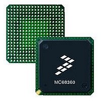
MC68EN360CAI25L Freescale Semiconductor, MC68EN360CAI25L Datasheet - Page 403

MC68EN360CAI25L
Manufacturer Part Number
MC68EN360CAI25L
Description
IC MPU QUICC 25MHZ 240-FQFP
Manufacturer
Freescale Semiconductor
Series
MC68000r
Datasheets
1.MC68EN302AG20BT.pdf
(8 pages)
2.MC68EN360VR25L.pdf
(14 pages)
3.MC68EN360VR25L.pdf
(2 pages)
4.MC68EN360CAI25L.pdf
(962 pages)
Specifications of MC68EN360CAI25L
Processor Type
M683xx 32-Bit
Speed
25MHz
Voltage
5V
Mounting Type
Surface Mount
Package / Case
240-FQFP
Core Size
32 Bit
Cpu Speed
25MHz
Embedded Interface Type
SCP, TDM
Digital Ic Case Style
FQFP
No. Of Pins
240
Supply Voltage Range
4.75V To 5.25V
Rohs Compliant
Yes
Family Name
M68xxx
Device Core
ColdFire
Device Core Size
32b
Frequency (max)
25MHz
Instruction Set Architecture
RISC
Supply Voltage 1 (typ)
5V
Operating Supply Voltage (max)
5.25V
Operating Supply Voltage (min)
4.75V
Operating Temp Range
-40C to 85C
Operating Temperature Classification
Industrial
Mounting
Surface Mount
Pin Count
240
Package Type
FQFP
Lead Free Status / RoHS Status
Lead free / RoHS Compliant
Features
-
Lead Free Status / Rohs Status
Compliant
Available stocks
Company
Part Number
Manufacturer
Quantity
Price
Company:
Part Number:
MC68EN360CAI25L
Manufacturer:
APLHA
Quantity:
12 000
Company:
Part Number:
MC68EN360CAI25L
Manufacturer:
Freescale Semiconductor
Quantity:
10 000
Part Number:
MC68EN360CAI25L
Manufacturer:
FREESCALE
Quantity:
20 000
- MC68EN302AG20BT PDF datasheet
- MC68EN360VR25L PDF datasheet #2
- MC68EN360VR25L PDF datasheet #3
- MC68EN360CAI25L PDF datasheet #4
- Current page: 403 of 962
- Download datasheet (4Mb)
SMC2CS—SMC2 Clock Source (NMSI mode)
SMC1CS—SMC1 Clock Source (NMSI mode)
SDMx—SI Diagnostic Mode for TDM A or B
SMC2 can take its clocks from one of the baud rate generators or one of four pins from
the bank of clocks. The SMC2 transmit and receive clocks must be the same when it is
connected to the NMSI.
SMC1 can take its clocks from one of the baud rate generators or one of four pins from
the bank of clocks. The SMC1 transmit and receive clocks must be the same when it is
connected to the NMSI.
000 = SMC2 transmit and receive clocks are BRG1.
001 = SMC2 transmit and receive clocks are BRG2.
010 = SMC2 transmit and receive clocks are BRG3.
011 = SMC2 transmit and receive clocks are BRG4.
100 = SMC2 transmit and receive clocks are CLK5.
101 = SMC2 transmit and receive clocks are CLK6.
110 = SMC2 transmit and receive clocks are CLK7.
111 = SMC2 transmit and receive clocks are CLK8.
000 = SMC1 transmit and receive clocks are BRG1.
001 = SMC1 transmit and receive clocks are BRG2.
010 = SMC1 transmit and receive clocks are BRG3.
011 = SMC1 transmit and receive clocks are BRG4.
100 = SMC1 transmit and receive clocks are CLK1.
101 = SMC1 transmit and receive clocks are CLK2.
110 = SMC1 transmit and receive clocks are CLK3.
111 = SMC1 transmit and receive clocks are CLK4.
00 = Normal operation.
01 = Automatic Echo. In this mode, the channel_x transmitter automatically retransmits
10 = Internal Loopback. In this mode, the TDM transmitter output is internally connect-
11 = Loopback Control. In this mode, the TDM transmitter output is internally connect-
the TDM received data on a bit-by-bit basis. The receive section operates normal-
ly, but the transmit section can only retransmit received data. In this mode, the
L1GRx line is ignored.
ed to the TDM receiver input (L1TXDx is connected to L1RXDx). The receiver and
transmitter operate normally. The data appears on the L1TXDx pin. In this mode,
the L1RQx line is asserted normally. The L1GRx line is ignored.
ed to the TDM receiver input (L1TXDx is connected to L1RXDx). The transmitter
output (L1TXDx) and the L1RQx pin will be inactive. This mode is used to accom-
plish loopback testing of the entire TDM without affecting the external serial lines.
In modes 01,10, and 11, the receive and the transmit clocks
should be identical.
Freescale Semiconductor, Inc.
For More Information On This Product,
MC68360 USER’S MANUAL
Go to: www.freescale.com
NOTE
Serial Interface with Time Slot Assigner
Related parts for MC68EN360CAI25L
Image
Part Number
Description
Manufacturer
Datasheet
Request
R
Part Number:
Description:
Manufacturer:
Freescale Semiconductor, Inc
Datasheet:
Part Number:
Description:
Manufacturer:
Freescale Semiconductor, Inc
Datasheet:
Part Number:
Description:
Manufacturer:
Freescale Semiconductor, Inc
Datasheet:
Part Number:
Description:
Manufacturer:
Freescale Semiconductor, Inc
Datasheet:
Part Number:
Description:
Manufacturer:
Freescale Semiconductor, Inc
Datasheet:
Part Number:
Description:
Manufacturer:
Freescale Semiconductor, Inc
Datasheet:
Part Number:
Description:
Manufacturer:
Freescale Semiconductor, Inc
Datasheet:
Part Number:
Description:
Manufacturer:
Freescale Semiconductor, Inc
Datasheet:
Part Number:
Description:
Manufacturer:
Freescale Semiconductor, Inc
Datasheet:
Part Number:
Description:
Manufacturer:
Freescale Semiconductor, Inc
Datasheet:
Part Number:
Description:
Manufacturer:
Freescale Semiconductor, Inc
Datasheet:
Part Number:
Description:
Manufacturer:
Freescale Semiconductor, Inc
Datasheet:
Part Number:
Description:
Manufacturer:
Freescale Semiconductor, Inc
Datasheet:
Part Number:
Description:
Manufacturer:
Freescale Semiconductor, Inc
Datasheet:
Part Number:
Description:
Manufacturer:
Freescale Semiconductor, Inc
Datasheet:


