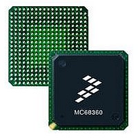
MC68EN360CAI25L Freescale Semiconductor, MC68EN360CAI25L Datasheet - Page 54

MC68EN360CAI25L
Manufacturer Part Number
MC68EN360CAI25L
Description
IC MPU QUICC 25MHZ 240-FQFP
Manufacturer
Freescale Semiconductor
Series
MC68000r
Datasheets
1.MC68EN302AG20BT.pdf
(8 pages)
2.MC68EN360VR25L.pdf
(14 pages)
3.MC68EN360VR25L.pdf
(2 pages)
4.MC68EN360CAI25L.pdf
(962 pages)
Specifications of MC68EN360CAI25L
Processor Type
M683xx 32-Bit
Speed
25MHz
Voltage
5V
Mounting Type
Surface Mount
Package / Case
240-FQFP
Core Size
32 Bit
Cpu Speed
25MHz
Embedded Interface Type
SCP, TDM
Digital Ic Case Style
FQFP
No. Of Pins
240
Supply Voltage Range
4.75V To 5.25V
Rohs Compliant
Yes
Family Name
M68xxx
Device Core
ColdFire
Device Core Size
32b
Frequency (max)
25MHz
Instruction Set Architecture
RISC
Supply Voltage 1 (typ)
5V
Operating Supply Voltage (max)
5.25V
Operating Supply Voltage (min)
4.75V
Operating Temp Range
-40C to 85C
Operating Temperature Classification
Industrial
Mounting
Surface Mount
Pin Count
240
Package Type
FQFP
Lead Free Status / RoHS Status
Lead free / RoHS Compliant
Features
-
Lead Free Status / Rohs Status
Compliant
Available stocks
Company
Part Number
Manufacturer
Quantity
Price
Company:
Part Number:
MC68EN360CAI25L
Manufacturer:
APLHA
Quantity:
12 000
Company:
Part Number:
MC68EN360CAI25L
Manufacturer:
Freescale Semiconductor
Quantity:
10 000
Part Number:
MC68EN360CAI25L
Manufacturer:
FREESCALE
Quantity:
20 000
- MC68EN302AG20BT PDF datasheet
- MC68EN360VR25L PDF datasheet #2
- MC68EN360VR25L PDF datasheet #3
- MC68EN360CAI25L PDF datasheet #4
- Current page: 54 of 962
- Download datasheet (4Mb)
Signal Descriptions
pins are the only data pins used. Refer to Section 4 Bus Operation for information on the
data bus and its relationship to bus operation.
2.1.3.2 DATA BUS (D15–D0). These pins can function as 16 additional data pins used in
long-word and 3-byte transfers. They are three-stated and not used if the QUICC is config-
ured into 16-bit bus mode.
2.1.4 Parity
These three-state bidirectional signals provide parity generation/checking for the data path
between the QUICC or external masters and other devices. There are four parity lines—one
for every eight data bits. The parity lines consists of two groups. Refer to Section 6 System
Integration Module (SIM60) for more information on parity generation/checking.
2.1.4.1 PARITY (PRTY0). This pin is the parity value for data bits 31–24.
2.1.4.2 PARITY (PRTY1). This pin is the parity value for data bits 23–16.
2.1.4.3 PARITY (PRTY2). This pin is the parity value for data bits 15–8.
2.1.4.4 PARITY (PRTY3). This pin has two functions. During total system reset, it is the
16BM pin to determine whether 16-bit data bus mode is to be enabled. After system reset,
it functions as the parity line 3.
PRTY3—This pin is the parity value for data bits 0–7.
16BM—This pin selects the 16-bit data bus mode. To choose a 32-bit data bus during total
system reset, this pin can be left floating (it has an internal pullup resistor) or can be driven/
pulled high. To choose a 16-bit data bus during total system reset, this pin should be driven/
pulled low.
2.1.5 Memory Controller
The following signals are used to control an external memory device.
2.1.5.1 CHIP SELECT/ROW ADDRESS SELECT (CS6–CS0/RAS6–RAS0). The
select output signals enable peripherals or memory arrays at programmed addresses. CS0
is the global chip select for the boot ROM containing the user’s reset vector and initialization
program. Refer to Section 6 System Integration Module (SIM60) for more information on
chip selects.
2.1.5.2 CHIP SELECT/ROW ADDRESS SELECT/INTERRUPT ACKNOWLEDGE (CS7/
RAS7/IACK7). This pin can be programmed as a CS7/RAS7 pin or as the IACK7 line. See
Section 6 System Integration Module (SIM60) for more information on this selection.
2-6
In addition, RAS1 can be simultaneously output on the RAS1DD
pin to increase the RAS1 line drive capability, and RAS2 can be
simultaneously output on the RAS2DD pin to increase the RAS2
line drive capability.
Freescale Semiconductor, Inc.
For More Information On This Product,
MC68360 USER’S MANUAL
Go to: www.freescale.com
NOTE
chip-
Related parts for MC68EN360CAI25L
Image
Part Number
Description
Manufacturer
Datasheet
Request
R
Part Number:
Description:
Manufacturer:
Freescale Semiconductor, Inc
Datasheet:
Part Number:
Description:
Manufacturer:
Freescale Semiconductor, Inc
Datasheet:
Part Number:
Description:
Manufacturer:
Freescale Semiconductor, Inc
Datasheet:
Part Number:
Description:
Manufacturer:
Freescale Semiconductor, Inc
Datasheet:
Part Number:
Description:
Manufacturer:
Freescale Semiconductor, Inc
Datasheet:
Part Number:
Description:
Manufacturer:
Freescale Semiconductor, Inc
Datasheet:
Part Number:
Description:
Manufacturer:
Freescale Semiconductor, Inc
Datasheet:
Part Number:
Description:
Manufacturer:
Freescale Semiconductor, Inc
Datasheet:
Part Number:
Description:
Manufacturer:
Freescale Semiconductor, Inc
Datasheet:
Part Number:
Description:
Manufacturer:
Freescale Semiconductor, Inc
Datasheet:
Part Number:
Description:
Manufacturer:
Freescale Semiconductor, Inc
Datasheet:
Part Number:
Description:
Manufacturer:
Freescale Semiconductor, Inc
Datasheet:
Part Number:
Description:
Manufacturer:
Freescale Semiconductor, Inc
Datasheet:
Part Number:
Description:
Manufacturer:
Freescale Semiconductor, Inc
Datasheet:
Part Number:
Description:
Manufacturer:
Freescale Semiconductor, Inc
Datasheet:


