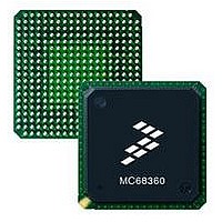
MC68EN360CAI25L Freescale Semiconductor, MC68EN360CAI25L Datasheet - Page 293

MC68EN360CAI25L
Manufacturer Part Number
MC68EN360CAI25L
Description
IC MPU QUICC 25MHZ 240-FQFP
Manufacturer
Freescale Semiconductor
Series
MC68000r
Datasheets
1.MC68EN302AG20BT.pdf
(8 pages)
2.MC68EN360VR25L.pdf
(14 pages)
3.MC68EN360VR25L.pdf
(2 pages)
4.MC68EN360CAI25L.pdf
(962 pages)
Specifications of MC68EN360CAI25L
Processor Type
M683xx 32-Bit
Speed
25MHz
Voltage
5V
Mounting Type
Surface Mount
Package / Case
240-FQFP
Core Size
32 Bit
Cpu Speed
25MHz
Embedded Interface Type
SCP, TDM
Digital Ic Case Style
FQFP
No. Of Pins
240
Supply Voltage Range
4.75V To 5.25V
Rohs Compliant
Yes
Family Name
M68xxx
Device Core
ColdFire
Device Core Size
32b
Frequency (max)
25MHz
Instruction Set Architecture
RISC
Supply Voltage 1 (typ)
5V
Operating Supply Voltage (max)
5.25V
Operating Supply Voltage (min)
4.75V
Operating Temp Range
-40C to 85C
Operating Temperature Classification
Industrial
Mounting
Surface Mount
Pin Count
240
Package Type
FQFP
Lead Free Status / RoHS Status
Lead free / RoHS Compliant
Features
-
Lead Free Status / Rohs Status
Compliant
Available stocks
Company
Part Number
Manufacturer
Quantity
Price
Company:
Part Number:
MC68EN360CAI25L
Manufacturer:
APLHA
Quantity:
12 000
Company:
Part Number:
MC68EN360CAI25L
Manufacturer:
Freescale Semiconductor
Quantity:
10 000
Part Number:
MC68EN360CAI25L
Manufacturer:
FREESCALE
Quantity:
20 000
- MC68EN302AG20BT PDF datasheet
- MC68EN360VR25L PDF datasheet #2
- MC68EN360VR25L PDF datasheet #3
- MC68EN360CAI25L PDF datasheet #4
- Current page: 293 of 962
- Download datasheet (4Mb)
Bits 14–12—SINTOUT
Bits 10–9—CF1MODE
Bit 8—IPIPE1/RAS1DD
Bit 7—A31–A28/WE0–WE3
Bit 6—OE/AMUX
These bits should only be modified from its default when the QUICC is configured in slave
(disable CPU32+) mode. They are used to program the way the interrupt controller will
assert its interrupt requests to the external logic.
These bits are used to control the CONFIG1/BCLRO/RAS2DD pin functionality.
000 = Default (Used only in CPU enable mode).
001 = Reserved.
010 = The QUICC interrupt request is the RQOUT output function on the IRQ1 pin.
011 = The QUICC interrupt request is the IOUT2–IOUT0 outputs with the standard
100 = The QUICC interrupt request is the RQOUT output function on the PRTY2 pin.
101 = The QUICC interrupt request is the IOUT2–IOUT0 outputs with the standard
110 = Reserved.
111 = Reserved.
00 = CONFIG1 input pin function is chosen.
01 = CONFIG1 input pin function is chosen.
10 = The BCLRO output function is chosen instead of the CONFIG1 pin.
11 = RAS2DD output function (RAS2 double-drive) is chosen instead of the CONFIG1
0 = If the QUICC is in normal mode, the IPIPE1 output function is selected. If the
1 = The RAS1DD output function (RAS1 double-drive) is selected.
0 = The A31–A28 input/output functions are selected.
1 = The WE0–WE3 output functions are selected.
0 = The OE output function is selected.
1 = The AMUX output function is selected.
QUICC is in slave mode, the BCLRI input function is selected.
pin.
M68000 family interrupt level encoding on the IRQ6, IRQ4, and IRQ1 pin, re-
spectively.
M68000 family interrupt level encoding on the PRTY0–PRTY2 pins, respective-
ly.
Until the low byte of PEPAR is written, the parity lines will be
three-stated. The user should write the high byte of PEPAR at
the same time that the low byte is written to avoid selecting a re-
served combination of the SINTOUT bits.
Until the low byte of PEPAR is written, the WE3–WE0/A31-28
pins are three-stated.
Freescale Semiconductor, Inc.
For More Information On This Product,
MC68360 USER’S MANUAL
Go to: www.freescale.com
NOTE
NOTE
System Integration Module (SIM60)
Related parts for MC68EN360CAI25L
Image
Part Number
Description
Manufacturer
Datasheet
Request
R
Part Number:
Description:
Manufacturer:
Freescale Semiconductor, Inc
Datasheet:
Part Number:
Description:
Manufacturer:
Freescale Semiconductor, Inc
Datasheet:
Part Number:
Description:
Manufacturer:
Freescale Semiconductor, Inc
Datasheet:
Part Number:
Description:
Manufacturer:
Freescale Semiconductor, Inc
Datasheet:
Part Number:
Description:
Manufacturer:
Freescale Semiconductor, Inc
Datasheet:
Part Number:
Description:
Manufacturer:
Freescale Semiconductor, Inc
Datasheet:
Part Number:
Description:
Manufacturer:
Freescale Semiconductor, Inc
Datasheet:
Part Number:
Description:
Manufacturer:
Freescale Semiconductor, Inc
Datasheet:
Part Number:
Description:
Manufacturer:
Freescale Semiconductor, Inc
Datasheet:
Part Number:
Description:
Manufacturer:
Freescale Semiconductor, Inc
Datasheet:
Part Number:
Description:
Manufacturer:
Freescale Semiconductor, Inc
Datasheet:
Part Number:
Description:
Manufacturer:
Freescale Semiconductor, Inc
Datasheet:
Part Number:
Description:
Manufacturer:
Freescale Semiconductor, Inc
Datasheet:
Part Number:
Description:
Manufacturer:
Freescale Semiconductor, Inc
Datasheet:
Part Number:
Description:
Manufacturer:
Freescale Semiconductor, Inc
Datasheet:


