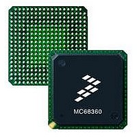
MC68EN360CAI25L Freescale Semiconductor, MC68EN360CAI25L Datasheet - Page 454

MC68EN360CAI25L
Manufacturer Part Number
MC68EN360CAI25L
Description
IC MPU QUICC 25MHZ 240-FQFP
Manufacturer
Freescale Semiconductor
Series
MC68000r
Datasheets
1.MC68EN302AG20BT.pdf
(8 pages)
2.MC68EN360VR25L.pdf
(14 pages)
3.MC68EN360VR25L.pdf
(2 pages)
4.MC68EN360CAI25L.pdf
(962 pages)
Specifications of MC68EN360CAI25L
Processor Type
M683xx 32-Bit
Speed
25MHz
Voltage
5V
Mounting Type
Surface Mount
Package / Case
240-FQFP
Core Size
32 Bit
Cpu Speed
25MHz
Embedded Interface Type
SCP, TDM
Digital Ic Case Style
FQFP
No. Of Pins
240
Supply Voltage Range
4.75V To 5.25V
Rohs Compliant
Yes
Family Name
M68xxx
Device Core
ColdFire
Device Core Size
32b
Frequency (max)
25MHz
Instruction Set Architecture
RISC
Supply Voltage 1 (typ)
5V
Operating Supply Voltage (max)
5.25V
Operating Supply Voltage (min)
4.75V
Operating Temp Range
-40C to 85C
Operating Temperature Classification
Industrial
Mounting
Surface Mount
Pin Count
240
Package Type
FQFP
Lead Free Status / RoHS Status
Lead free / RoHS Compliant
Features
-
Lead Free Status / Rohs Status
Compliant
Available stocks
Company
Part Number
Manufacturer
Quantity
Price
Company:
Part Number:
MC68EN360CAI25L
Manufacturer:
APLHA
Quantity:
12 000
Company:
Part Number:
MC68EN360CAI25L
Manufacturer:
Freescale Semiconductor
Quantity:
10 000
Part Number:
MC68EN360CAI25L
Manufacturer:
FREESCALE
Quantity:
20 000
- MC68EN302AG20BT PDF datasheet
- MC68EN360VR25L PDF datasheet #2
- MC68EN360VR25L PDF datasheet #3
- MC68EN360CAI25L PDF datasheet #4
- Current page: 454 of 962
- Download datasheet (4Mb)
Serial Communication Controllers (SCCs)
any dynamic change in its parallel I/O ports or serial channel physical interface configura-
tion. A full reset using the RST bit in the CR is a comprehensive reset that may also be used.
7.10.10 SCC Interrupt Handling
The following describes what would normally take place within an interrupt handler for the
SCC.
7.10.11 SCC Timing Control
When the DIAG bits of the GSMR are programmed to normal operation, the CD and CTS
lines are controlled automatically by the SCC. The following paragraphs describe the behav-
ior in this mode. In the following description, the TCI bit in the GSMR is assumed to be
cleared, implying normal transmit clock operation.
7.10.11.1 SYNCHRONOUS PROTOCOLS. The RTS pin is asserted when the SCC data is
loaded into the transmit FIFO and a falling transmit clock occurs. At this point, the SCC
begins transmitting the data, once the appropriate conditions occur on the CTS pin. In all
cases, the first bit of data is the first bit of the opening flag, sync pattern, or the preamble (if
a preamble was programmed to be sent prior to the frame).
Figure 7-39 shows that the delay between RTS and data is 0 bit times, regardless of the
CTSS bit in the GSMR. This operation assumes that the CTS pin is already asserted to the
SCC or that the CTS pin is reprogrammed to be a parallel I/O line, in which case the CTS
signal to the SCC is always asserted. RTS is negated one clock after the last bit in the frame.
7-130
1. Once an interrupt occurs, the SCCE should be read by the user to see which sources
2. Process the Tx BDs to reuse them if the TX bit or TXE bit was set in SCCE. If the trans-
3. Extract data from the Rx BD if the RX, RXB, or RXF bit was set in SCCE. If the receive
4. Clear the SCCx bit in the CISR.
5. Execute the RTE instruction.
have caused interrupts. The SCCE bits that are going to be "handled" in this interrupt
handler would normally be cleared at this time.
mit speed is fast or the interrupt delay is long, more than one transmit buffer may have
been sent by the SCC. Thus, it is important to check more than just one Tx BD during
the interrupt handler. One common practice is to process all Tx BDs in the interrupt
handler until one is found with its R-bit set.
speed is fast or the interrupt delay is long, more than one receive buffer may have
been received by the SCC. Thus, it is important to check more than just one Rx BD
during the interrupt handler. One common practice is to process all Rx BDs in the in-
terrupt handler until one is found with its E-bit set.
Freescale Semiconductor, Inc.
For More Information On This Product,
MC68360 USER’S MANUAL
Go to: www.freescale.com
Related parts for MC68EN360CAI25L
Image
Part Number
Description
Manufacturer
Datasheet
Request
R
Part Number:
Description:
Manufacturer:
Freescale Semiconductor, Inc
Datasheet:
Part Number:
Description:
Manufacturer:
Freescale Semiconductor, Inc
Datasheet:
Part Number:
Description:
Manufacturer:
Freescale Semiconductor, Inc
Datasheet:
Part Number:
Description:
Manufacturer:
Freescale Semiconductor, Inc
Datasheet:
Part Number:
Description:
Manufacturer:
Freescale Semiconductor, Inc
Datasheet:
Part Number:
Description:
Manufacturer:
Freescale Semiconductor, Inc
Datasheet:
Part Number:
Description:
Manufacturer:
Freescale Semiconductor, Inc
Datasheet:
Part Number:
Description:
Manufacturer:
Freescale Semiconductor, Inc
Datasheet:
Part Number:
Description:
Manufacturer:
Freescale Semiconductor, Inc
Datasheet:
Part Number:
Description:
Manufacturer:
Freescale Semiconductor, Inc
Datasheet:
Part Number:
Description:
Manufacturer:
Freescale Semiconductor, Inc
Datasheet:
Part Number:
Description:
Manufacturer:
Freescale Semiconductor, Inc
Datasheet:
Part Number:
Description:
Manufacturer:
Freescale Semiconductor, Inc
Datasheet:
Part Number:
Description:
Manufacturer:
Freescale Semiconductor, Inc
Datasheet:
Part Number:
Description:
Manufacturer:
Freescale Semiconductor, Inc
Datasheet:


