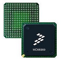
MC68EN360CAI25L Freescale Semiconductor, MC68EN360CAI25L Datasheet - Page 207

MC68EN360CAI25L
Manufacturer Part Number
MC68EN360CAI25L
Description
IC MPU QUICC 25MHZ 240-FQFP
Manufacturer
Freescale Semiconductor
Series
MC68000r
Datasheets
1.MC68EN302AG20BT.pdf
(8 pages)
2.MC68EN360VR25L.pdf
(14 pages)
3.MC68EN360VR25L.pdf
(2 pages)
4.MC68EN360CAI25L.pdf
(962 pages)
Specifications of MC68EN360CAI25L
Processor Type
M683xx 32-Bit
Speed
25MHz
Voltage
5V
Mounting Type
Surface Mount
Package / Case
240-FQFP
Core Size
32 Bit
Cpu Speed
25MHz
Embedded Interface Type
SCP, TDM
Digital Ic Case Style
FQFP
No. Of Pins
240
Supply Voltage Range
4.75V To 5.25V
Rohs Compliant
Yes
Family Name
M68xxx
Device Core
ColdFire
Device Core Size
32b
Frequency (max)
25MHz
Instruction Set Architecture
RISC
Supply Voltage 1 (typ)
5V
Operating Supply Voltage (max)
5.25V
Operating Supply Voltage (min)
4.75V
Operating Temp Range
-40C to 85C
Operating Temperature Classification
Industrial
Mounting
Surface Mount
Pin Count
240
Package Type
FQFP
Lead Free Status / RoHS Status
Lead free / RoHS Compliant
Features
-
Lead Free Status / Rohs Status
Compliant
Available stocks
Company
Part Number
Manufacturer
Quantity
Price
Company:
Part Number:
MC68EN360CAI25L
Manufacturer:
APLHA
Quantity:
12 000
Company:
Part Number:
MC68EN360CAI25L
Manufacturer:
Freescale Semiconductor
Quantity:
10 000
Part Number:
MC68EN360CAI25L
Manufacturer:
FREESCALE
Quantity:
20 000
- MC68EN302AG20BT PDF datasheet
- MC68EN360VR25L PDF datasheet #2
- MC68EN360VR25L PDF datasheet #3
- MC68EN360CAI25L PDF datasheet #4
- Current page: 207 of 962
- Download datasheet (4Mb)
5.6.2.7.1 CPU Serial Logic. CPU32+ serial logic, shown in the left-hand portion of Figure
5-22, consists of transmit and receive shift registers and of control logic that includes syn-
chronization, serial clock generation circuitry, and a received bit counter.
Both DSCLK and DSI are synchronized to on-chip clocks, thereby minimizing the chance of
propagating metastable states into the serial state machine. Data is sampled during the high
phase of CLKOUT. At the falling edge of CLKOUT, the sampled value is made available to
internal logic. If there is no synchronization between CPU32+ and development system
hardware, the minimum hold time on DSI with respect to DSCLK is one full period of CLK-
OUT.
The serial state machine begins a sequence of events based on the rising edge of the syn-
chronized DSCLK (see Figure 5-23). Synchronized serial data is transferred to the input shift
register, and the received bit counter is decremented. One-half clock period later, the output
shift register is updated, bringing the next output bit to the DSO signal. DSO changes rela-
tive to the rising edge of DSCLK and does not necessarily remain stable until the falling edge
of DSCLK.
One clock period after the synchronized DSCLK has been seen internally, the updated
counter value is checked. If the counter has reached zero, the receive data latch is updated
from the input shift register. At this same time, the output shift register is reloaded with the
MICROSEQUENCER
SYNCHRONIZE
EXECUTION
STATUS
UNIT
Figure 5-22. Debug Serial I/O Block Diagram
Freescale Semiconductor, Inc.
For More Information On This Product,
RCV DATA LATCH
PARALLEL OUT
REGISTER BUS
PARALLEL IN
INSTRUCTION
SERIAL OUT
SERIAL IN
MC68360 USER’S MANUAL
Go to: www.freescale.com
CPU
16
16
CONTROL
LOGIC
DSCLK
DSO
DSI
STATUS
0
DEVELOPMENT SYSTEM
COMMAND LATCH
PARALLEL OUT
RESULT LATCH
CONTROL
PARALLEL IN
SERIAL OUT
LOGIC
SERIAL IN
DATA
DATA
16
16
SERIAL
CLOCK
CPU32+
Related parts for MC68EN360CAI25L
Image
Part Number
Description
Manufacturer
Datasheet
Request
R
Part Number:
Description:
Manufacturer:
Freescale Semiconductor, Inc
Datasheet:
Part Number:
Description:
Manufacturer:
Freescale Semiconductor, Inc
Datasheet:
Part Number:
Description:
Manufacturer:
Freescale Semiconductor, Inc
Datasheet:
Part Number:
Description:
Manufacturer:
Freescale Semiconductor, Inc
Datasheet:
Part Number:
Description:
Manufacturer:
Freescale Semiconductor, Inc
Datasheet:
Part Number:
Description:
Manufacturer:
Freescale Semiconductor, Inc
Datasheet:
Part Number:
Description:
Manufacturer:
Freescale Semiconductor, Inc
Datasheet:
Part Number:
Description:
Manufacturer:
Freescale Semiconductor, Inc
Datasheet:
Part Number:
Description:
Manufacturer:
Freescale Semiconductor, Inc
Datasheet:
Part Number:
Description:
Manufacturer:
Freescale Semiconductor, Inc
Datasheet:
Part Number:
Description:
Manufacturer:
Freescale Semiconductor, Inc
Datasheet:
Part Number:
Description:
Manufacturer:
Freescale Semiconductor, Inc
Datasheet:
Part Number:
Description:
Manufacturer:
Freescale Semiconductor, Inc
Datasheet:
Part Number:
Description:
Manufacturer:
Freescale Semiconductor, Inc
Datasheet:
Part Number:
Description:
Manufacturer:
Freescale Semiconductor, Inc
Datasheet:


