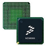
MC68EN360CAI25L Freescale Semiconductor, MC68EN360CAI25L Datasheet - Page 398

MC68EN360CAI25L
Manufacturer Part Number
MC68EN360CAI25L
Description
IC MPU QUICC 25MHZ 240-FQFP
Manufacturer
Freescale Semiconductor
Series
MC68000r
Datasheets
1.MC68EN302AG20BT.pdf
(8 pages)
2.MC68EN360VR25L.pdf
(14 pages)
3.MC68EN360VR25L.pdf
(2 pages)
4.MC68EN360CAI25L.pdf
(962 pages)
Specifications of MC68EN360CAI25L
Processor Type
M683xx 32-Bit
Speed
25MHz
Voltage
5V
Mounting Type
Surface Mount
Package / Case
240-FQFP
Core Size
32 Bit
Cpu Speed
25MHz
Embedded Interface Type
SCP, TDM
Digital Ic Case Style
FQFP
No. Of Pins
240
Supply Voltage Range
4.75V To 5.25V
Rohs Compliant
Yes
Family Name
M68xxx
Device Core
ColdFire
Device Core Size
32b
Frequency (max)
25MHz
Instruction Set Architecture
RISC
Supply Voltage 1 (typ)
5V
Operating Supply Voltage (max)
5.25V
Operating Supply Voltage (min)
4.75V
Operating Temp Range
-40C to 85C
Operating Temperature Classification
Industrial
Mounting
Surface Mount
Pin Count
240
Package Type
FQFP
Lead Free Status / RoHS Status
Lead free / RoHS Compliant
Features
-
Lead Free Status / Rohs Status
Compliant
Available stocks
Company
Part Number
Manufacturer
Quantity
Price
Company:
Part Number:
MC68EN360CAI25L
Manufacturer:
APLHA
Quantity:
12 000
Company:
Part Number:
MC68EN360CAI25L
Manufacturer:
Freescale Semiconductor
Quantity:
10 000
Part Number:
MC68EN360CAI25L
Manufacturer:
FREESCALE
Quantity:
20 000
- MC68EN302AG20BT PDF datasheet
- MC68EN360VR25L PDF datasheet #2
- MC68EN360VR25L PDF datasheet #3
- MC68EN360CAI25L PDF datasheet #4
- Current page: 398 of 962
- Download datasheet (4Mb)
Serial Interface with Time Slot Assigner
CSEL—Channel Select
CNT—Count
BYT—Byte Resolution
LST—Last Entry in the RAM
7-74
This value indicates the number of bits/bytes (according to the BYT bit) that the routing
and strobe select of this entry controls. If CNT = 0000, then 1 bit/byte is chosen; if
CNT = 1111, then 16 bits/bytes are selected.
Whenever the SI RAM is used, this bit must be set in one of the Tx or Rx entries of each
group that is used. Even if all entries of a group are used, this bit must still be set in the
last entry.
000 = The bit/byte group is not supported within the QUICC. The transmit data pin is
001 = The bit/byte group is routed to SCC1.
010 = The bit/byte group is routed to SCC2.
011 = The bit/byte group is routed to SCC3.
100 = The bit/byte group is routed to SCC4.
101 = The bit/byte group is routed to SMC1.
110 = The bit/byte group is routed to SMC2.
111 = The bit/byte group is not supported within the QUICC. This code is also used in
0 = Bit resolution—the CNT value indicates the number of bits in this group.
1 = Byte resolution—the CNT value indicates the number of bytes in this group.
0 = This is not the last entry in this section of the route RAM.
1 = This is the last entry in this RAM. After this entry, the SI will wait for the sync signal
to start the next frame.
three-stated, and the receive data pin is ignored.
SCIT mode as the D channel grant (refer to 7.8.7.2.2 SCIT Programming.)
Each strobe is changed with the corresponding RAM clock and
will be output only if the corresponding parallel I/O is configured
as a dedicated pin.
If a strobe is programmed to be asserted in more than one set of
entries (e.g., the SI Rx route for the TDMa entries and the SI Tx
route for TDMb entries both select the same strobe), then the as-
sertion of the strobe corresponds to the logical OR of all possible
sources. This use of the strobes is not useful for most applica-
tions. It is recommended that a given strobe be selected in only
one set of SI RAM entries.
If a second sync signal is received before the end of a frame (as
defined by the last SI RAM entry), an error occurs. The SI will ter-
minate SI RAM processing, and cease transmitting or receiving
data until a third sync signal is received.
Freescale Semiconductor, Inc.
For More Information On This Product,
MC68360 USER’S MANUAL
Go to: www.freescale.com
NOTES
NOTE
Related parts for MC68EN360CAI25L
Image
Part Number
Description
Manufacturer
Datasheet
Request
R
Part Number:
Description:
Manufacturer:
Freescale Semiconductor, Inc
Datasheet:
Part Number:
Description:
Manufacturer:
Freescale Semiconductor, Inc
Datasheet:
Part Number:
Description:
Manufacturer:
Freescale Semiconductor, Inc
Datasheet:
Part Number:
Description:
Manufacturer:
Freescale Semiconductor, Inc
Datasheet:
Part Number:
Description:
Manufacturer:
Freescale Semiconductor, Inc
Datasheet:
Part Number:
Description:
Manufacturer:
Freescale Semiconductor, Inc
Datasheet:
Part Number:
Description:
Manufacturer:
Freescale Semiconductor, Inc
Datasheet:
Part Number:
Description:
Manufacturer:
Freescale Semiconductor, Inc
Datasheet:
Part Number:
Description:
Manufacturer:
Freescale Semiconductor, Inc
Datasheet:
Part Number:
Description:
Manufacturer:
Freescale Semiconductor, Inc
Datasheet:
Part Number:
Description:
Manufacturer:
Freescale Semiconductor, Inc
Datasheet:
Part Number:
Description:
Manufacturer:
Freescale Semiconductor, Inc
Datasheet:
Part Number:
Description:
Manufacturer:
Freescale Semiconductor, Inc
Datasheet:
Part Number:
Description:
Manufacturer:
Freescale Semiconductor, Inc
Datasheet:
Part Number:
Description:
Manufacturer:
Freescale Semiconductor, Inc
Datasheet:


