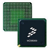
MC68EN360CAI25L Freescale Semiconductor, MC68EN360CAI25L Datasheet - Page 781

MC68EN360CAI25L
Manufacturer Part Number
MC68EN360CAI25L
Description
IC MPU QUICC 25MHZ 240-FQFP
Manufacturer
Freescale Semiconductor
Series
MC68000r
Datasheets
1.MC68EN302AG20BT.pdf
(8 pages)
2.MC68EN360VR25L.pdf
(14 pages)
3.MC68EN360VR25L.pdf
(2 pages)
4.MC68EN360CAI25L.pdf
(962 pages)
Specifications of MC68EN360CAI25L
Processor Type
M683xx 32-Bit
Speed
25MHz
Voltage
5V
Mounting Type
Surface Mount
Package / Case
240-FQFP
Core Size
32 Bit
Cpu Speed
25MHz
Embedded Interface Type
SCP, TDM
Digital Ic Case Style
FQFP
No. Of Pins
240
Supply Voltage Range
4.75V To 5.25V
Rohs Compliant
Yes
Family Name
M68xxx
Device Core
ColdFire
Device Core Size
32b
Frequency (max)
25MHz
Instruction Set Architecture
RISC
Supply Voltage 1 (typ)
5V
Operating Supply Voltage (max)
5.25V
Operating Supply Voltage (min)
4.75V
Operating Temp Range
-40C to 85C
Operating Temperature Classification
Industrial
Mounting
Surface Mount
Pin Count
240
Package Type
FQFP
Lead Free Status / RoHS Status
Lead free / RoHS Compliant
Features
-
Lead Free Status / Rohs Status
Compliant
Available stocks
Company
Part Number
Manufacturer
Quantity
Price
Company:
Part Number:
MC68EN360CAI25L
Manufacturer:
APLHA
Quantity:
12 000
Company:
Part Number:
MC68EN360CAI25L
Manufacturer:
Freescale Semiconductor
Quantity:
10 000
Part Number:
MC68EN360CAI25L
Manufacturer:
FREESCALE
Quantity:
20 000
- MC68EN302AG20BT PDF datasheet
- MC68EN360VR25L PDF datasheet #2
- MC68EN360VR25L PDF datasheet #3
- MC68EN360CAI25L PDF datasheet #4
- Current page: 781 of 962
- Download datasheet (4Mb)
Applications
9.6.4 Functional Description
The 53C90 SCSI controller consists of three major sections: the processor interface, the
data path, and the logic block. The processor interface includes the 8-bit data bus, parity bit,
chip select, read/write strobes, A0–A3 address lines, interrupt request, and DMA signals.
The data path consists of a 16-byte FIFO, parity generation, DMA interface, and SCSI data
and control bus inputs/outputs.
The logic block consists of a hierarchy of sequencers that direct the SCSI bus control signal
timing. The 53C90 has a set of on-chip state machines that directly perform many SCSI
sequences. The instruction sequencer and master sequencer provide control of these state
machines. Since the 53C90 has no real decision-making capability, it relies on the CPU32+
for supervisory control and for integrating the performed SCSI sequences into complete
operations. Processor service is requested through a standard interrupt structure, and the
53C90 reports the status through its register set.
Overall control of the 53C90 is done through the processor interface. The processor data
bus and associated control signals provide the means to initialize and set the operating
mode of the SCSI as well as provide the data path for information swapping. The processor
can write to a set of 12 registers, instructing the 53C90 what function to perform, then read
another set of registers to determine the status.
Once the 53C90 starts executing, all data transfers are handled by the DMA. Since the
53C90 does not have an onboard DMA controller, it relies on one of the two independent
DMA (IDMA) channels of the QUICC. In this case, IDMA1 is arbitrarily chosen. IDMA1 of the
QUICC moves the data to and from the 53C90 FIFO. The FIFO provides a 9-bit-wide by 16-
byte-deep buffer. It can be accessed by either the IDMA or the processor at register address
$02 and can be read or written as a register. The bottom of the FIFO is read and unloaded
while the top is written to and loaded.
Therefore, for an SCSI transfer to occur, the processor has to initialize the 53C90 by writing
to its registers, initialize IDMA1 by setting up its registers, and then monitor the status of the
53C90.
Table 9-2 lists the read and write registers in the 53C90.
9-61
Address (Hex)
$0C-$0F
$0A
$0B
$00
$01
$03
$04
$05
$06
$07
$08
$09
$02
Table 9-3. 53C90 Read and Write Registers
Freescale Semiconductor, Inc.
For More Information On This Product,
MC68360 USER’S MANUAL
Transfer Counter MSB
Go to: www.freescale.com
Transfer Counter LSB
FIFO Flags/Seq. Step
Instruction Executing
Sequence Step
Configuration 1
Configuration 2
Read Register
Reserved
Reserved
Reserved
Interrupt
Status
FIFO
Clock Conversion (Presel)
Select/Reselect Timeout
Transfer Counter MSB
Transfer Counter LSB
Synchronous Period
Synchronous Offset
Instruction Holding
Write Register
Configuration 1
Configuration 2
Destination ID
Test Mode
Reserved
FIFO
Related parts for MC68EN360CAI25L
Image
Part Number
Description
Manufacturer
Datasheet
Request
R
Part Number:
Description:
Manufacturer:
Freescale Semiconductor, Inc
Datasheet:
Part Number:
Description:
Manufacturer:
Freescale Semiconductor, Inc
Datasheet:
Part Number:
Description:
Manufacturer:
Freescale Semiconductor, Inc
Datasheet:
Part Number:
Description:
Manufacturer:
Freescale Semiconductor, Inc
Datasheet:
Part Number:
Description:
Manufacturer:
Freescale Semiconductor, Inc
Datasheet:
Part Number:
Description:
Manufacturer:
Freescale Semiconductor, Inc
Datasheet:
Part Number:
Description:
Manufacturer:
Freescale Semiconductor, Inc
Datasheet:
Part Number:
Description:
Manufacturer:
Freescale Semiconductor, Inc
Datasheet:
Part Number:
Description:
Manufacturer:
Freescale Semiconductor, Inc
Datasheet:
Part Number:
Description:
Manufacturer:
Freescale Semiconductor, Inc
Datasheet:
Part Number:
Description:
Manufacturer:
Freescale Semiconductor, Inc
Datasheet:
Part Number:
Description:
Manufacturer:
Freescale Semiconductor, Inc
Datasheet:
Part Number:
Description:
Manufacturer:
Freescale Semiconductor, Inc
Datasheet:
Part Number:
Description:
Manufacturer:
Freescale Semiconductor, Inc
Datasheet:
Part Number:
Description:
Manufacturer:
Freescale Semiconductor, Inc
Datasheet:


