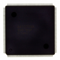
D6417729RHF200BV Renesas Electronics America, D6417729RHF200BV Datasheet - Page 94

D6417729RHF200BV
Manufacturer Part Number
D6417729RHF200BV
Description
IC SUPER H MPU ROMLESS 208QFP
Manufacturer
Renesas Electronics America
Series
SuperH® SH7700r
Datasheet
1.D6417729RF133BV.pdf
(857 pages)
Specifications of D6417729RHF200BV
Core Processor
SH-3 DSP
Core Size
32-Bit
Speed
200MHz
Connectivity
EBI/EMI, FIFO, IrDA, SCI, SmartCard
Peripherals
DMA, POR, WDT
Number Of I /o
96
Program Memory Type
ROMless
Ram Size
32K x 8
Voltage - Supply (vcc/vdd)
1.85 V ~ 2.15 V
Data Converters
A/D 8x10b; D/A 2x8b
Oscillator Type
Internal
Operating Temperature
-20°C ~ 75°C
Package / Case
208-QFP Exposed Pad, 208-eQFP, 208-HQFP
Lead Free Status / RoHS Status
Lead free / RoHS Compliant
Eeprom Size
-
Program Memory Size
-
Available stocks
Company
Part Number
Manufacturer
Quantity
Price
Company:
Part Number:
D6417729RHF200BV
Manufacturer:
EVERLIGHT
Quantity:
1 000
Company:
Part Number:
D6417729RHF200BV
Manufacturer:
Renesas Electronics America
Quantity:
10 000
- Current page: 94 of 857
- Download datasheet (5Mb)
3. Increment address register addressing:
There is an index register for each address pointer. The R8 register is the index register (Ix) for the
X memory address register (Ax), and the R9 register is the index register (Iy) for the Y memory
address register (Ay).
The X and Y data transfer instructions perform word-length processing, and use 16-bit access to
the X/Y data memory. A value of 2 is therefore added to the address register in the increment
processing. To perform decrementing, –2 is set in the index register and addition index register
addressing is specified. In X/Y data addressing, only bits 1 to 15 of the address pointer are valid.
When using X/Y data addressing, 0 must always be written to bit 0 of the address pointer and
index register.
X/Y data transfer addressing is shown in figure 2.12. When accessing X and Y memory using the
X and Y buses, the upper word of Ax (R4 or R5) and Ay (R6 or R7) is ignored. The result of
@AY+ or @Ay+Iy is stored in the lower word of Ay, while the upper word retains its original
value.
Single Data Addressing: DSP instructions include two single data transfer instructions
(MOVS.W, MOVS.L) that load data into, or store data from, a DSP register. With these
instructions, one of registers R2 to R5 is used as the single data transfer address register (As).
The following four kinds of addressing can be used with single data transfer instructions.
Rev. 5.0, 09/03, page 46 of 806
The Ax and Ay registers are address pointers. After a data transfer, they are each incremented
by 2 (post-increment).
Note: Three address processing methods:
+2 (INC)
+0 (no update)
1. Increment
2. Index register addition (Ix/Iy)
3. No increment
Post-updating is used in all cases.
The address pointer can be decremented by setting −2/−4 in the index register.
R8[Ix]
Figure 2.12 X and Y Data Transfer Addressing
ALU
R4[Ax]
R5[Ax]
+2 (INC)
+0 (no update)
R9[Iy]
AU: Adder provided
AU
for DSP addressing
R6[Ay]
R7[Ay]
Related parts for D6417729RHF200BV
Image
Part Number
Description
Manufacturer
Datasheet
Request
R

Part Number:
Description:
KIT STARTER FOR M16C/29
Manufacturer:
Renesas Electronics America
Datasheet:

Part Number:
Description:
KIT STARTER FOR R8C/2D
Manufacturer:
Renesas Electronics America
Datasheet:

Part Number:
Description:
R0K33062P STARTER KIT
Manufacturer:
Renesas Electronics America
Datasheet:

Part Number:
Description:
KIT STARTER FOR R8C/23 E8A
Manufacturer:
Renesas Electronics America
Datasheet:

Part Number:
Description:
KIT STARTER FOR R8C/25
Manufacturer:
Renesas Electronics America
Datasheet:

Part Number:
Description:
KIT STARTER H8S2456 SHARPE DSPLY
Manufacturer:
Renesas Electronics America
Datasheet:

Part Number:
Description:
KIT STARTER FOR R8C38C
Manufacturer:
Renesas Electronics America
Datasheet:

Part Number:
Description:
KIT STARTER FOR R8C35C
Manufacturer:
Renesas Electronics America
Datasheet:

Part Number:
Description:
KIT STARTER FOR R8CL3AC+LCD APPS
Manufacturer:
Renesas Electronics America
Datasheet:

Part Number:
Description:
KIT STARTER FOR RX610
Manufacturer:
Renesas Electronics America
Datasheet:

Part Number:
Description:
KIT STARTER FOR R32C/118
Manufacturer:
Renesas Electronics America
Datasheet:

Part Number:
Description:
KIT DEV RSK-R8C/26-29
Manufacturer:
Renesas Electronics America
Datasheet:

Part Number:
Description:
KIT STARTER FOR SH7124
Manufacturer:
Renesas Electronics America
Datasheet:

Part Number:
Description:
KIT STARTER FOR H8SX/1622
Manufacturer:
Renesas Electronics America
Datasheet:

Part Number:
Description:
KIT DEV FOR SH7203
Manufacturer:
Renesas Electronics America
Datasheet:


