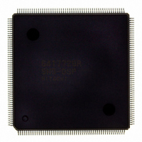
D6417729RHF200BV Renesas Electronics America, D6417729RHF200BV Datasheet - Page 142

D6417729RHF200BV
Manufacturer Part Number
D6417729RHF200BV
Description
IC SUPER H MPU ROMLESS 208QFP
Manufacturer
Renesas Electronics America
Series
SuperH® SH7700r
Datasheet
1.D6417729RF133BV.pdf
(857 pages)
Specifications of D6417729RHF200BV
Core Processor
SH-3 DSP
Core Size
32-Bit
Speed
200MHz
Connectivity
EBI/EMI, FIFO, IrDA, SCI, SmartCard
Peripherals
DMA, POR, WDT
Number Of I /o
96
Program Memory Type
ROMless
Ram Size
32K x 8
Voltage - Supply (vcc/vdd)
1.85 V ~ 2.15 V
Data Converters
A/D 8x10b; D/A 2x8b
Oscillator Type
Internal
Operating Temperature
-20°C ~ 75°C
Package / Case
208-QFP Exposed Pad, 208-eQFP, 208-HQFP
Lead Free Status / RoHS Status
Lead free / RoHS Compliant
Eeprom Size
-
Program Memory Size
-
Available stocks
Company
Part Number
Manufacturer
Quantity
Price
Company:
Part Number:
D6417729RHF200BV
Manufacturer:
EVERLIGHT
Quantity:
1 000
Company:
Part Number:
D6417729RHF200BV
Manufacturer:
Renesas Electronics America
Quantity:
10 000
- Current page: 142 of 857
- Download datasheet (5Mb)
3.1.3
SH7729R MMU
Virtual Address Space: The SH7729R uses 32-bit virtual addresses to access a 4-Gbyte virtual
address space that is divided into several areas. Address space mapping is shown in figure 3.2.
(a) Privileged Mode
In privileged mode, there are five areas, P0–P4. The P0 and P3 areas are mapped onto physical
address space in page units, in accordance with address translation table information. Write-back
or write-through can be selected for write access by means of a cache control register (CCR)
setting.
Mapping of the P1 area is fixed in physical address space (H'00000000 to H'1FFFFFFF). In the
P1 area, setting a virtual address MSB (bit 31) to 0 generates the corresponding physical address.
P1 area accesses can be cached, and the cache control register (CCR) is set to indicate whether to
cache or not. Write-back or write-through mode can be selected.
Mapping of the P2 area is fixed in physical address space (H'00000000 to H'1FFFFFFF). In the P2
area, setting the top three virtual address bits (bits 31, 30, and 29) to 0 generates the corresponding
physical address. P2 area access cannot be cached.
The P1 and P2 areas are not mapped by the address translation table, so the TLB is not used and
no exceptions such as TLB misses occur. Initialization of MMU control registers, exception
handling routines, and the like should be located in the P1 and P2 areas. Routines that require
high-speed processing should be placed in the P1 area, since it can be cached.
Some peripheral module control registers are located in area 1 of the physical address space. When
the physical address space is not used for address translation, these registers should be located in
the P2 area. When address translation is to be used, set no caching.
The P4 area is used for mapping peripheral module register addresses, etc.
(b) User Mode
In user mode, 2 Gbytes of the virtual address space from H'00000000 to H'7FFFFFFF (area U0)
can be accessed. U0 is mapped onto physical address space in page units, in accordance with
address translation table information. When the DSP bit in CPU status register (SR) is off, 2
Gbytes of the virtual address space from H'80000000 to H'FFFFFFFF cannot be accessed in the
user mode. Attempting to do so creates an address error. Write-back or write-through mode can
be selected for write accesses by means of a cache control register (CCR) setting. When the DSP
bit in CPU status register (SR) is on, a new 16-Mbyte address space, Uxy, is defined from address
H'A5000000 to H'A5FFFFFF for X/Y RAM. This Uxy space is non-cached, fixed physical
address space. Any access to address space beyond U0 and Uxy creates an address error. For
details of the X/Y RAM space, refer to section 6, X/Y Memory.
Rev. 5.0, 09/03, page 94 of 806
Related parts for D6417729RHF200BV
Image
Part Number
Description
Manufacturer
Datasheet
Request
R

Part Number:
Description:
KIT STARTER FOR M16C/29
Manufacturer:
Renesas Electronics America
Datasheet:

Part Number:
Description:
KIT STARTER FOR R8C/2D
Manufacturer:
Renesas Electronics America
Datasheet:

Part Number:
Description:
R0K33062P STARTER KIT
Manufacturer:
Renesas Electronics America
Datasheet:

Part Number:
Description:
KIT STARTER FOR R8C/23 E8A
Manufacturer:
Renesas Electronics America
Datasheet:

Part Number:
Description:
KIT STARTER FOR R8C/25
Manufacturer:
Renesas Electronics America
Datasheet:

Part Number:
Description:
KIT STARTER H8S2456 SHARPE DSPLY
Manufacturer:
Renesas Electronics America
Datasheet:

Part Number:
Description:
KIT STARTER FOR R8C38C
Manufacturer:
Renesas Electronics America
Datasheet:

Part Number:
Description:
KIT STARTER FOR R8C35C
Manufacturer:
Renesas Electronics America
Datasheet:

Part Number:
Description:
KIT STARTER FOR R8CL3AC+LCD APPS
Manufacturer:
Renesas Electronics America
Datasheet:

Part Number:
Description:
KIT STARTER FOR RX610
Manufacturer:
Renesas Electronics America
Datasheet:

Part Number:
Description:
KIT STARTER FOR R32C/118
Manufacturer:
Renesas Electronics America
Datasheet:

Part Number:
Description:
KIT DEV RSK-R8C/26-29
Manufacturer:
Renesas Electronics America
Datasheet:

Part Number:
Description:
KIT STARTER FOR SH7124
Manufacturer:
Renesas Electronics America
Datasheet:

Part Number:
Description:
KIT STARTER FOR H8SX/1622
Manufacturer:
Renesas Electronics America
Datasheet:

Part Number:
Description:
KIT DEV FOR SH7203
Manufacturer:
Renesas Electronics America
Datasheet:


