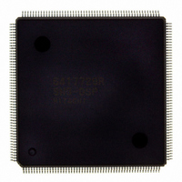
D6417729RHF200BV Renesas Electronics America, D6417729RHF200BV Datasheet - Page 194

D6417729RHF200BV
Manufacturer Part Number
D6417729RHF200BV
Description
IC SUPER H MPU ROMLESS 208QFP
Manufacturer
Renesas Electronics America
Series
SuperH® SH7700r
Datasheet
1.D6417729RF133BV.pdf
(857 pages)
Specifications of D6417729RHF200BV
Core Processor
SH-3 DSP
Core Size
32-Bit
Speed
200MHz
Connectivity
EBI/EMI, FIFO, IrDA, SCI, SmartCard
Peripherals
DMA, POR, WDT
Number Of I /o
96
Program Memory Type
ROMless
Ram Size
32K x 8
Voltage - Supply (vcc/vdd)
1.85 V ~ 2.15 V
Data Converters
A/D 8x10b; D/A 2x8b
Oscillator Type
Internal
Operating Temperature
-20°C ~ 75°C
Package / Case
208-QFP Exposed Pad, 208-eQFP, 208-HQFP
Lead Free Status / RoHS Status
Lead free / RoHS Compliant
Eeprom Size
-
Program Memory Size
-
Available stocks
Company
Part Number
Manufacturer
Quantity
Price
Company:
Part Number:
D6417729RHF200BV
Manufacturer:
EVERLIGHT
Quantity:
1 000
Company:
Part Number:
D6417729RHF200BV
Manufacturer:
Renesas Electronics America
Quantity:
10 000
- Current page: 194 of 857
- Download datasheet (5Mb)
5.2.2
CCR2 register is used to enable or disable the cache locking mechanism in DSP mode (set by CPU
status register bit 12) only. Executing a prefetch instruction (PREF) in DSP mode will bring the
line of data pointed to by Rn into the cache, according to the setting of CCR2 [9:8] (W3LOAD,
W3LOCK) and [1:0] (W2LOAD, W2LOCK).
When CCR2[9:8]=11, in DSP mode PREF @Rn will bring the data into way 3. When
CCR2[9:8]=00, 01, or 10 in DSP mode, or any setting in non-DSP mode, PREF @Rn will place
the data into the way pointed to by LRU.
When CCR2[1:0]=11, in DSP mode PREF @Rn will bring the data into way 2. When
CCR2[1:0]=00, 01, or 10 in DSP mode, or any setting in non-DSP mode, PREF @Rn will place
the data into the way pointed to by LRU.
CCR2 must be set before the cache is enabled (CCR.CE = 1).
When a PREF instruction is issued and there is a cache hit, the operation is treated as NOP.
Figure 5.3 shows the configuration of the CCR2 register.
CCR2 is a write-only register; if read, an undefined value will be returned.
Rev. 5.0, 09/03, page 146 of 806
Bits 5, 4: Always set to 0 when setting the register.
CF:
CB:
WT:
CE:
31
Cache Control Register 2 (CCR2)
…
Cache flush bit. Writing 1 flushes all cache entries (clears the V, U, and LRU bits of all
cache entries to 0). Always reads 0. Write-back to external memory is not performed when
the cache is flushed.
Cache write-back bit. Indicates the cache's operating mode for area P1.
1 = write-back mode, 0 = write-through mode.
Write-through bit. Indicates the cache's operating mode for areas P0, U0, and P3.
1 = write-through mode, 0 = write-back mode.
Cache enable bit. Indicates whether the cache function is used.
1 = cache used, 0 = cache not used.
…
…
Figure 5.2 CCR Register Configuration
…
…
…
…
…
6
0
5
0
4
CF
3
CB
2
WT
1
CE
0
Related parts for D6417729RHF200BV
Image
Part Number
Description
Manufacturer
Datasheet
Request
R

Part Number:
Description:
KIT STARTER FOR M16C/29
Manufacturer:
Renesas Electronics America
Datasheet:

Part Number:
Description:
KIT STARTER FOR R8C/2D
Manufacturer:
Renesas Electronics America
Datasheet:

Part Number:
Description:
R0K33062P STARTER KIT
Manufacturer:
Renesas Electronics America
Datasheet:

Part Number:
Description:
KIT STARTER FOR R8C/23 E8A
Manufacturer:
Renesas Electronics America
Datasheet:

Part Number:
Description:
KIT STARTER FOR R8C/25
Manufacturer:
Renesas Electronics America
Datasheet:

Part Number:
Description:
KIT STARTER H8S2456 SHARPE DSPLY
Manufacturer:
Renesas Electronics America
Datasheet:

Part Number:
Description:
KIT STARTER FOR R8C38C
Manufacturer:
Renesas Electronics America
Datasheet:

Part Number:
Description:
KIT STARTER FOR R8C35C
Manufacturer:
Renesas Electronics America
Datasheet:

Part Number:
Description:
KIT STARTER FOR R8CL3AC+LCD APPS
Manufacturer:
Renesas Electronics America
Datasheet:

Part Number:
Description:
KIT STARTER FOR RX610
Manufacturer:
Renesas Electronics America
Datasheet:

Part Number:
Description:
KIT STARTER FOR R32C/118
Manufacturer:
Renesas Electronics America
Datasheet:

Part Number:
Description:
KIT DEV RSK-R8C/26-29
Manufacturer:
Renesas Electronics America
Datasheet:

Part Number:
Description:
KIT STARTER FOR SH7124
Manufacturer:
Renesas Electronics America
Datasheet:

Part Number:
Description:
KIT STARTER FOR H8SX/1622
Manufacturer:
Renesas Electronics America
Datasheet:

Part Number:
Description:
KIT DEV FOR SH7203
Manufacturer:
Renesas Electronics America
Datasheet:


