D6417729RHF200BV Renesas Electronics America, D6417729RHF200BV Datasheet - Page 13
D6417729RHF200BV
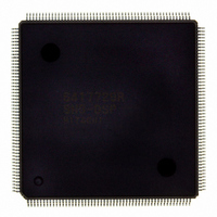
Manufacturer Part Number
D6417729RHF200BV
Description
IC SUPER H MPU ROMLESS 208QFP
Manufacturer
Renesas Electronics America
Series
SuperH® SH7700r
Datasheet
1.D6417729RF133BV.pdf
(857 pages)
Specifications of D6417729RHF200BV
Core Processor
SH-3 DSP
Core Size
32-Bit
Speed
200MHz
Connectivity
EBI/EMI, FIFO, IrDA, SCI, SmartCard
Peripherals
DMA, POR, WDT
Number Of I /o
96
Program Memory Type
ROMless
Ram Size
32K x 8
Voltage - Supply (vcc/vdd)
1.85 V ~ 2.15 V
Data Converters
A/D 8x10b; D/A 2x8b
Oscillator Type
Internal
Operating Temperature
-20°C ~ 75°C
Package / Case
208-QFP Exposed Pad, 208-eQFP, 208-HQFP
Lead Free Status / RoHS Status
Lead free / RoHS Compliant
Eeprom Size
-
Program Memory Size
-
Available stocks
Company
Part Number
Manufacturer
Quantity
Price
Company:

Part Number:
D6417729RHF200BV
Manufacturer:
EVERLIGHT
Quantity:
1 000
Company:
Part Number:
D6417729RHF200BV
Manufacturer:
Renesas Electronics America
Quantity:
10 000


Section
5.5.1 Invalidating a
Specific Entry
5.5.2 Invalidating a
Specific Address
5.5.3 Reading the
Data of a Specific Entry
7.2.6 Interrupt
Exception Handling and
Priority
Table 7.4 Interrupt
Exception Handling
Sources and Priority
(IRQ Mode)
7.3.6 Interrupt
Request Register 0
(IRR0)
9.2.1 Standby Control
Register (STBCR)
Page
154
155
171
182
230
Description
Description amended
A specific cache entry can be invalidated by accessing the allocated
memory cache and writing a 0 to the entry’s U and V bits. The A bit is
cleared to 0, and an address is specified for the entry address and the
way. If the U bit of the way of the entry in question was set to 1, the
entry is written back and the V and U bits specified by the write data are
written to.
In the following example, the write data is specified in R0 and the
address is specified in R1.
; R0 = H'0000 0000 LRU = H'000, U = 0, V = 0
; R1 = H'F000 1080, Way = 1, Entry = H'08, A = 0
;
To invalidate all entries and ways, write 0 to the following addresses.
This involves a total of 1,024 writes.
The above operation should be performed using a non-cacheable area.
Newly added
Description amended
; R1=H'F100 004C; data array access, entry=H'04, Way = 0,
; longword address = 3
;
MOV.L @R0,R1 ; Longword 3 is read.
IPR (bit numbers) for SCI amended
(Before)IPRB(3-0)
Description amended
When clearing an IRQ5R–IRQ0R bit to 0, read the bit while bit set
to 1, and then write 0. In this case, 0 should be written only to the
bits to be cleared and 1 to the other bits. The contents of the bits
to which 1 is written do not change.
Description added
Bit 1—Module Standby 1 (MSTP1)
Before switching the RTC to module standby, access at least one
among the registers RTC, SCI, and TMU.
MOV.L R0, @R1
Addresses
F000 0000
F000 0010
F000 0020
F000 3FF0
:
(After)IPRB(7-4)
Rev. 5.0, 09/03, page xi of xlvi
Related parts for D6417729RHF200BV
Image
Part Number
Description
Manufacturer
Datasheet
Request
R

Part Number:
Description:
KIT STARTER FOR M16C/29
Manufacturer:
Renesas Electronics America
Datasheet:

Part Number:
Description:
KIT STARTER FOR R8C/2D
Manufacturer:
Renesas Electronics America
Datasheet:

Part Number:
Description:
R0K33062P STARTER KIT
Manufacturer:
Renesas Electronics America
Datasheet:

Part Number:
Description:
KIT STARTER FOR R8C/23 E8A
Manufacturer:
Renesas Electronics America
Datasheet:

Part Number:
Description:
KIT STARTER FOR R8C/25
Manufacturer:
Renesas Electronics America
Datasheet:

Part Number:
Description:
KIT STARTER H8S2456 SHARPE DSPLY
Manufacturer:
Renesas Electronics America
Datasheet:

Part Number:
Description:
KIT STARTER FOR R8C38C
Manufacturer:
Renesas Electronics America
Datasheet:

Part Number:
Description:
KIT STARTER FOR R8C35C
Manufacturer:
Renesas Electronics America
Datasheet:

Part Number:
Description:
KIT STARTER FOR R8CL3AC+LCD APPS
Manufacturer:
Renesas Electronics America
Datasheet:
Part Number:
Description:
KIT STARTER FOR RX610
Manufacturer:
Renesas Electronics America
Datasheet:

Part Number:
Description:
KIT STARTER FOR R32C/118
Manufacturer:
Renesas Electronics America
Datasheet:

Part Number:
Description:
KIT DEV RSK-R8C/26-29
Manufacturer:
Renesas Electronics America
Datasheet:

Part Number:
Description:
KIT STARTER FOR SH7124
Manufacturer:
Renesas Electronics America
Datasheet:

Part Number:
Description:
KIT STARTER FOR H8SX/1622
Manufacturer:
Renesas Electronics America
Datasheet:

Part Number:
Description:
KIT DEV FOR SH7203
Manufacturer:
Renesas Electronics America
Datasheet: