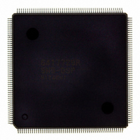
D6417729RHF200BV Renesas Electronics America, D6417729RHF200BV Datasheet - Page 567

D6417729RHF200BV
Manufacturer Part Number
D6417729RHF200BV
Description
IC SUPER H MPU ROMLESS 208QFP
Manufacturer
Renesas Electronics America
Series
SuperH® SH7700r
Datasheet
1.D6417729RF133BV.pdf
(857 pages)
Specifications of D6417729RHF200BV
Core Processor
SH-3 DSP
Core Size
32-Bit
Speed
200MHz
Connectivity
EBI/EMI, FIFO, IrDA, SCI, SmartCard
Peripherals
DMA, POR, WDT
Number Of I /o
96
Program Memory Type
ROMless
Ram Size
32K x 8
Voltage - Supply (vcc/vdd)
1.85 V ~ 2.15 V
Data Converters
A/D 8x10b; D/A 2x8b
Oscillator Type
Internal
Operating Temperature
-20°C ~ 75°C
Package / Case
208-QFP Exposed Pad, 208-eQFP, 208-HQFP
Lead Free Status / RoHS Status
Lead free / RoHS Compliant
Eeprom Size
-
Program Memory Size
-
Available stocks
Company
Part Number
Manufacturer
Quantity
Price
Company:
Part Number:
D6417729RHF200BV
Manufacturer:
EVERLIGHT
Quantity:
1 000
Company:
Part Number:
D6417729RHF200BV
Manufacturer:
Renesas Electronics America
Quantity:
10 000
- Current page: 567 of 857
- Download datasheet (5Mb)
Clock: An internal clock generated by the on-chip baud rate generator or an external clock input
from the SCK pin can be selected as the SCI transmit/receive clock. The clock source is selected
by the C/A bit in the serial mode register (SCSMR) and bits CKE1 and CKE0 in the serial control
register (SCSCR). See table 15.10.
When the SCI operates on an internal clock, it outputs the clock signal at the SCK pin. Eight clock
pulses are output per transmitted or received character. When the SCI is not transmitting or
receiving, the clock signal remains in the high state. When only receiving, the SCI receives in 2-
character units, so a 16-pulse serial clock is output. To receive in 1-character units, select an
external clock source.
Transmitting and Receiving Data SCI Initialization (Synchronous Mode): Before
transmitting, receiving, or changing the mode or communication format, the software must clear
the TE and RE bits to 0 in the serial control register (SCSCR), then initialize the SCI. Clearing TE
to 0 sets TDRE to 1 and initializes the transmit shift register (SCTSR). Clearing RE to 0, however,
does not initialize the RDRF, PER, FER, and ORER flags and receive data register (SCRDR),
which retain their previous contents.
Figure 15.18 shows a sample flowchart for initializing the SCI. The procedure for initializing the
SCI is:
1. Select the clock source in the serial control register (SCSCR). Leave RIE, TIE, TEIE, MPIE,
2. Select the communication format in the serial mode register (SCSMR).
3. Write the value corresponding to the bit rate in the bit rate register (SCBRR) (not necessary if
4. Wait for at least the interval required to transmit or receive one bit, then set TE or RE in the
TE and RE cleared to 0.
an external clock is used).
serial control register (SCSCR) to 1. Also set RIE, TIE, TEIE and MPIE. Setting TE and RE
allows use of the TxD and RxD pins.
Rev. 5.0, 09/03, page 519 of 806
Related parts for D6417729RHF200BV
Image
Part Number
Description
Manufacturer
Datasheet
Request
R

Part Number:
Description:
KIT STARTER FOR M16C/29
Manufacturer:
Renesas Electronics America
Datasheet:

Part Number:
Description:
KIT STARTER FOR R8C/2D
Manufacturer:
Renesas Electronics America
Datasheet:

Part Number:
Description:
R0K33062P STARTER KIT
Manufacturer:
Renesas Electronics America
Datasheet:

Part Number:
Description:
KIT STARTER FOR R8C/23 E8A
Manufacturer:
Renesas Electronics America
Datasheet:

Part Number:
Description:
KIT STARTER FOR R8C/25
Manufacturer:
Renesas Electronics America
Datasheet:

Part Number:
Description:
KIT STARTER H8S2456 SHARPE DSPLY
Manufacturer:
Renesas Electronics America
Datasheet:

Part Number:
Description:
KIT STARTER FOR R8C38C
Manufacturer:
Renesas Electronics America
Datasheet:

Part Number:
Description:
KIT STARTER FOR R8C35C
Manufacturer:
Renesas Electronics America
Datasheet:

Part Number:
Description:
KIT STARTER FOR R8CL3AC+LCD APPS
Manufacturer:
Renesas Electronics America
Datasheet:

Part Number:
Description:
KIT STARTER FOR RX610
Manufacturer:
Renesas Electronics America
Datasheet:

Part Number:
Description:
KIT STARTER FOR R32C/118
Manufacturer:
Renesas Electronics America
Datasheet:

Part Number:
Description:
KIT DEV RSK-R8C/26-29
Manufacturer:
Renesas Electronics America
Datasheet:

Part Number:
Description:
KIT STARTER FOR SH7124
Manufacturer:
Renesas Electronics America
Datasheet:

Part Number:
Description:
KIT STARTER FOR H8SX/1622
Manufacturer:
Renesas Electronics America
Datasheet:

Part Number:
Description:
KIT DEV FOR SH7203
Manufacturer:
Renesas Electronics America
Datasheet:


