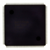
D6417729RHF200BV Renesas Electronics America, D6417729RHF200BV Datasheet - Page 323

D6417729RHF200BV
Manufacturer Part Number
D6417729RHF200BV
Description
IC SUPER H MPU ROMLESS 208QFP
Manufacturer
Renesas Electronics America
Series
SuperH® SH7700r
Datasheet
1.D6417729RF133BV.pdf
(857 pages)
Specifications of D6417729RHF200BV
Core Processor
SH-3 DSP
Core Size
32-Bit
Speed
200MHz
Connectivity
EBI/EMI, FIFO, IrDA, SCI, SmartCard
Peripherals
DMA, POR, WDT
Number Of I /o
96
Program Memory Type
ROMless
Ram Size
32K x 8
Voltage - Supply (vcc/vdd)
1.85 V ~ 2.15 V
Data Converters
A/D 8x10b; D/A 2x8b
Oscillator Type
Internal
Operating Temperature
-20°C ~ 75°C
Package / Case
208-QFP Exposed Pad, 208-eQFP, 208-HQFP
Lead Free Status / RoHS Status
Lead free / RoHS Compliant
Eeprom Size
-
Program Memory Size
-
Available stocks
Company
Part Number
Manufacturer
Quantity
Price
Company:
Part Number:
D6417729RHF200BV
Manufacturer:
EVERLIGHT
Quantity:
1 000
Company:
Part Number:
D6417729RHF200BV
Manufacturer:
Renesas Electronics America
Quantity:
10 000
- Current page: 323 of 857
- Download datasheet (5Mb)
11.1.5
Space Allocation: In the architecture of the SH7729R, both logical spaces and physical spaces
have 32-bit address spaces. The logical space is divided into five areas by the value of the upper
bits of the address. The physical space is divided into eight areas.
Logical space can be allocated to physical space using a memory management unit (MMU). For
details, refer to section 3, Memory Management Unit (MMU), which describes area allocation for
physical space.
As shown in table 11.3, the SH7729R can be connected directly to six memory/PCMCIA interface
areas, and it outputs chip select signals (CS0, CS2–CS6, CE2A, CE2B) for each of them. CS0 is
asserted during area 0 access; CS6 is asserted during area 6 access. When PCMCIA interface is
selected in area 5 or 6, in addition to CS5/CS6, CE2A/CE2B are asserted for the corresponding
bytes accessed.
Figure 11.2 Correspondence between Logical Address Space and Physical Address Space
H'C0000000
H'A0000000
H'E0000000
Note: For logical address spaces P0 and P3, when the memory management unit (MMU) is
H'00000000
H'20000000
H'40000000
H'60000000
H'80000000
on, it can optionally generate a physical address for the logical address. This diagram
can be applied when the MMU is off, and when the MMU is on and each physical
address corresponding to a logical address is equal except for the upper three bits.
When translating logical addresses to arbitrary physical addresses, refer to table 11.3.
Area Overview
Logical address space
P0, U0
P1
P2
P3
P4
Physical address space
Rev. 5.0, 09/03, page 275 of 806
Reserved area
Area 0 (CS0)
Area 2 (CS2)
Area 3 (CS3)
Area 4 (CS4)
Area 5 (CS5)
Area 6 (CS6)
Internal I/O
H'00000000
H'04000000
H'08000000
H'0C000000
H'10000000
H'14000000
H'18000000
Related parts for D6417729RHF200BV
Image
Part Number
Description
Manufacturer
Datasheet
Request
R

Part Number:
Description:
KIT STARTER FOR M16C/29
Manufacturer:
Renesas Electronics America
Datasheet:

Part Number:
Description:
KIT STARTER FOR R8C/2D
Manufacturer:
Renesas Electronics America
Datasheet:

Part Number:
Description:
R0K33062P STARTER KIT
Manufacturer:
Renesas Electronics America
Datasheet:

Part Number:
Description:
KIT STARTER FOR R8C/23 E8A
Manufacturer:
Renesas Electronics America
Datasheet:

Part Number:
Description:
KIT STARTER FOR R8C/25
Manufacturer:
Renesas Electronics America
Datasheet:

Part Number:
Description:
KIT STARTER H8S2456 SHARPE DSPLY
Manufacturer:
Renesas Electronics America
Datasheet:

Part Number:
Description:
KIT STARTER FOR R8C38C
Manufacturer:
Renesas Electronics America
Datasheet:

Part Number:
Description:
KIT STARTER FOR R8C35C
Manufacturer:
Renesas Electronics America
Datasheet:

Part Number:
Description:
KIT STARTER FOR R8CL3AC+LCD APPS
Manufacturer:
Renesas Electronics America
Datasheet:

Part Number:
Description:
KIT STARTER FOR RX610
Manufacturer:
Renesas Electronics America
Datasheet:

Part Number:
Description:
KIT STARTER FOR R32C/118
Manufacturer:
Renesas Electronics America
Datasheet:

Part Number:
Description:
KIT DEV RSK-R8C/26-29
Manufacturer:
Renesas Electronics America
Datasheet:

Part Number:
Description:
KIT STARTER FOR SH7124
Manufacturer:
Renesas Electronics America
Datasheet:

Part Number:
Description:
KIT STARTER FOR H8SX/1622
Manufacturer:
Renesas Electronics America
Datasheet:

Part Number:
Description:
KIT DEV FOR SH7203
Manufacturer:
Renesas Electronics America
Datasheet:


