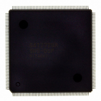
D6417729RHF200BV Renesas Electronics America, D6417729RHF200BV Datasheet - Page 369

D6417729RHF200BV
Manufacturer Part Number
D6417729RHF200BV
Description
IC SUPER H MPU ROMLESS 208QFP
Manufacturer
Renesas Electronics America
Series
SuperH® SH7700r
Datasheet
1.D6417729RF133BV.pdf
(857 pages)
Specifications of D6417729RHF200BV
Core Processor
SH-3 DSP
Core Size
32-Bit
Speed
200MHz
Connectivity
EBI/EMI, FIFO, IrDA, SCI, SmartCard
Peripherals
DMA, POR, WDT
Number Of I /o
96
Program Memory Type
ROMless
Ram Size
32K x 8
Voltage - Supply (vcc/vdd)
1.85 V ~ 2.15 V
Data Converters
A/D 8x10b; D/A 2x8b
Oscillator Type
Internal
Operating Temperature
-20°C ~ 75°C
Package / Case
208-QFP Exposed Pad, 208-eQFP, 208-HQFP
Lead Free Status / RoHS Status
Lead free / RoHS Compliant
Eeprom Size
-
Program Memory Size
-
Available stocks
Company
Part Number
Manufacturer
Quantity
Price
Company:
Part Number:
D6417729RHF200BV
Manufacturer:
EVERLIGHT
Quantity:
1 000
Company:
Part Number:
D6417729RHF200BV
Manufacturer:
Renesas Electronics America
Quantity:
10 000
- Current page: 369 of 857
- Download datasheet (5Mb)
11.3.4
Synchronous DRAM Interface
Synchronous DRAM Direct Connection: Since synchronous DRAM can be selected by the CS
signal, physical space areas 2 and 3 can be connected using RAS and other control signals in
common. If the memory type bits (DRAMTP2–0) in BCR1 are set to 010, area 2 is ordinary
memory space and area 3 is synchronous DRAM space; if set to 011, areas 2 and 3 are both
synchronous DRAM space. Note, however, that synchronous DRAM must not be accessed when
clock ratio I :B = 1:1.
With the SH7729R, burst length 1 burst read/single write mode is supported as the synchronous
DRAM operating mode. A data bus width of 16 or 32 bits can be selected. The burst enable bit
(BE) in MCR is ignored, a 16-bit burst transfer is performed in a cache fill/write-back cycle, and
only one access is performed in a write-through area write or a non-cacheable area read/write.
The control signals for direct connection of synchronous DRAM are RAS3L, RAS3U, CASL,
CASU, RD/WR, CS2 or CS3, DQMUU, DQMUL, DQMLU, DQMLL, and CKE. All the signals
other than CS2 and CS3 are common to all areas, and signals other than CKE are valid and fetched
to the synchronous DRAM only when CS2 or CS3 is asserted. Synchronous DRAM can therefore
be connected in parallel to a number of areas. CKE is negated (low) only when self-refreshing is
performed, and is always asserted (high) at other times.
In the refresh cycle and mode-register write cycle, RAS3U and RAS3L or CASU and CASL are
output.
Commands for synchronous DRAM are specified by RAS3L, RAS3U, CASL, CASU, RD/WR,
and special address signals. The commands are NOP, auto-refresh (REF), self-refresh (SELF),
precharge all banks (PALL), row address strobe bank active (ACTV), read (READ), read with
precharge (READA), write (WRIT), write with precharge (WRITA), and mode register write
(MRS).
Byte specification is performed by DQMUU, DQMUL, DQMLU, and DQMLL. A read/write is
performed for the byte for which the corresponding DQM is low. In big-endian mode, DQMUU
specifies an access to address 4n, and DQMLL specifies an access to address 4n + 3. In little-
endian mode, DQMUU specifies an access to address 4n + 3, and DQMLL specifies an access to
address 4n.
Figures 11.12 and 11.13 show examples of the connection of two 1M 16-bit
4-bank
synchronous DRAMs and one 1M
16-bit
4-bank synchronous DRAM, respectively.
Rev. 5.0, 09/03, page 321 of 806
Related parts for D6417729RHF200BV
Image
Part Number
Description
Manufacturer
Datasheet
Request
R

Part Number:
Description:
KIT STARTER FOR M16C/29
Manufacturer:
Renesas Electronics America
Datasheet:

Part Number:
Description:
KIT STARTER FOR R8C/2D
Manufacturer:
Renesas Electronics America
Datasheet:

Part Number:
Description:
R0K33062P STARTER KIT
Manufacturer:
Renesas Electronics America
Datasheet:

Part Number:
Description:
KIT STARTER FOR R8C/23 E8A
Manufacturer:
Renesas Electronics America
Datasheet:

Part Number:
Description:
KIT STARTER FOR R8C/25
Manufacturer:
Renesas Electronics America
Datasheet:

Part Number:
Description:
KIT STARTER H8S2456 SHARPE DSPLY
Manufacturer:
Renesas Electronics America
Datasheet:

Part Number:
Description:
KIT STARTER FOR R8C38C
Manufacturer:
Renesas Electronics America
Datasheet:

Part Number:
Description:
KIT STARTER FOR R8C35C
Manufacturer:
Renesas Electronics America
Datasheet:

Part Number:
Description:
KIT STARTER FOR R8CL3AC+LCD APPS
Manufacturer:
Renesas Electronics America
Datasheet:

Part Number:
Description:
KIT STARTER FOR RX610
Manufacturer:
Renesas Electronics America
Datasheet:

Part Number:
Description:
KIT STARTER FOR R32C/118
Manufacturer:
Renesas Electronics America
Datasheet:

Part Number:
Description:
KIT DEV RSK-R8C/26-29
Manufacturer:
Renesas Electronics America
Datasheet:

Part Number:
Description:
KIT STARTER FOR SH7124
Manufacturer:
Renesas Electronics America
Datasheet:

Part Number:
Description:
KIT STARTER FOR H8SX/1622
Manufacturer:
Renesas Electronics America
Datasheet:

Part Number:
Description:
KIT DEV FOR SH7203
Manufacturer:
Renesas Electronics America
Datasheet:


