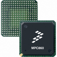
MC68360VR25VL Freescale Semiconductor, MC68360VR25VL Datasheet - Page 96

MC68360VR25VL
Manufacturer Part Number
MC68360VR25VL
Description
IC MPU QUICC 25MHZ 357-PBGA
Manufacturer
Freescale Semiconductor
Datasheets
1.MC68EN360VR25L.pdf
(14 pages)
2.MC68EN360VR25L.pdf
(2 pages)
3.MC68360AI25L.pdf
(962 pages)
Specifications of MC68360VR25VL
Processor Type
M683xx 32-Bit
Speed
25MHz
Voltage
3.3V
Mounting Type
Surface Mount
Package / Case
357-PBGA
Family Name
M68000
Device Core
ColdFire
Device Core Size
32b
Frequency (max)
25MHz
Instruction Set Architecture
RISC
Operating Supply Voltage (max)
3.3V
Operating Supply Voltage (min)
2.7V
Operating Temp Range
0C to 70C
Operating Temperature Classification
Commercial
Mounting
Surface Mount
Pin Count
357
Package Type
BGA
Lead Free Status / RoHS Status
Lead free / RoHS Compliant
Features
-
Lead Free Status / Rohs Status
Compliant
Available stocks
Company
Part Number
Manufacturer
Quantity
Price
Company:
Part Number:
MC68360VR25VL
Manufacturer:
Exar
Quantity:
160
Company:
Part Number:
MC68360VR25VL
Manufacturer:
Freescale Semiconductor
Quantity:
10 000
Company:
Part Number:
MC68360VR25VLR2
Manufacturer:
Freescale Semiconductor
Quantity:
10 000
- Current page: 96 of 962
- Download datasheet (4Mb)
Bus Operation
This table verifies that bus cycle throughput is significantly affected by port size and align-
ment. The QUICC system designer and programmer should be aware of and account for
these effects, particularly in time-critical applications.
If the required instruction begins at an even-word boundary, the processor prefetches a long
word (up to two instructions) by reading a long word from a long-word address (A1–A0 = 00),
regardless of port size. When the required instruction begins at an odd-word boundary, the
processor reads 16-bits only, from the odd-word boundary. Refer to Section 5 CPU32+ for
a complete description of the pipeline operation.
4.2.4 Bus Operation
The QUICC bus is asynchronous, allowing external devices connected to the bus to operate
at clock frequencies different from the clock for the QUICC. Bus operation uses the hand-
shake lines (AS, DS, DSACK1, DSACK0, BERR, and HALT) to control data transfers. AS
signals a valid address on the address bus, and DS is used as a condition for valid data on
a write cycle. Decoding the SIZx outputs and lower address lines (A1–A0) provides strobes
that select the active portion of the data bus. The slave device (memory or peripheral)
responds by placing the requested data on the correct portion of the data bus for a read
cycle or by latching the data on a write cycle; the slave asserts the DSACK1/DSACK0 com-
bination that corresponds to the port size to terminate the cycle.
Alternatively, the SIM60 can be programmed to assert the DSACK1/DSACK0 combination
internally and respond for the slave. If no slave responds or the access is invalid, external
control logic may assert BERR or BERR with HALT to abort or retry the bus cycle, respec-
tively. DSACKx can be asserted before the data from a slave device is valid on a read cycle.
The length of time that DSACKx may precede data must not exceed a specified value in any
asynchronous system to ensure that valid data is latched into the QUICC. (See Section 10
Electrical Characteristics for timing parameters.)
Note that no maximum time is specified from the assertion of AS to the assertion of
DSACKx. Although the QUICC can transfer data in a minimum of three clock cycles when
the cycle is terminated with DSACKx, the QUICC inserts wait cycles in clock-period incre-
ments until DSACKx is recognized. BERR and/or HALT can be asserted after DSACKx is
asserted. BERR and/or HALT must be asserted within the time specified after DSACKx is
4-20
Table 4-7. Memory Alignment and Port Size Influence
Notes:
1. Data Port Size—32 Bits:16 Bits:8 Bits
2. Instruction reads can either be two words from an
Instruction 1
Byte Operand
Word Operand
Long-Word Operand
even-word boundary, or one word from an odd-word boundary.
A1–A0
Freescale Semiconductor, Inc.
For More Information On This Product,
MC68360 USER’S MANUAL
on Write Bus Cycles
Go to: www.freescale.com
1:2:4
1:1:1
1:1:2
1:2:4
00
Number of Bus Cycles
1:1:1
1:2:2
2:3:4
N/A
01
1:1:1
1:1:2
2:2:4
N/A
10
1:1:1
2:2:2
2:3:4
N/A
11
Related parts for MC68360VR25VL
Image
Part Number
Description
Manufacturer
Datasheet
Request
R
Part Number:
Description:
Manufacturer:
Freescale Semiconductor, Inc
Datasheet:

Part Number:
Description:
MC68360 MC68360 Multiple Ethernet Channels on the QUICC
Manufacturer:
Motorola / Freescale Semiconductor

Part Number:
Description:
MC68360 Implementing an 8 bit Eprom for an MC68EC040-MC68360 System
Manufacturer:
Motorola / Freescale Semiconductor

Part Number:
Description:
MC68360 Interfacing the MC68060 to the MC68360
Manufacturer:
Motorola / Freescale Semiconductor

Part Number:
Description:
MC68360 MC68360 RAM Microcode Package Option Overview
Manufacturer:
Motorola / Freescale Semiconductor

Part Number:
Description:
MC68360 MC68360 CPM-CPU Interaction
Manufacturer:
Motorola / Freescale Semiconductor

Part Number:
Description:
MC68360 Interfacing SDRAM to the MC68360 QUICC Device
Manufacturer:
Motorola / Freescale Semiconductor

Part Number:
Description:
MC68360 Interfacing the QUICC to a MCM516400 (4Mx4 10-12 column-row) DRAM
Manufacturer:
Motorola / Freescale Semiconductor

Part Number:
Description:
MC68360 Interfacing the 68360 (QUICC) to T1-E1 Systems
Manufacturer:
Motorola / Freescale Semiconductor

Part Number:
Description:
MC68360 Multiple QUICC Design Concept
Manufacturer:
Motorola / Freescale Semiconductor
Part Number:
Description:
Manufacturer:
Freescale Semiconductor, Inc
Datasheet:
Part Number:
Description:
Manufacturer:
Freescale Semiconductor, Inc
Datasheet:
Part Number:
Description:
Manufacturer:
Freescale Semiconductor, Inc
Datasheet:
Part Number:
Description:
Manufacturer:
Freescale Semiconductor, Inc
Datasheet:
Part Number:
Description:
Manufacturer:
Freescale Semiconductor, Inc
Datasheet:


