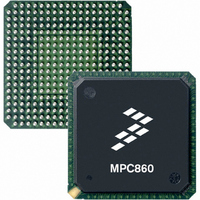
MC68360VR25VL Freescale Semiconductor, MC68360VR25VL Datasheet - Page 665

MC68360VR25VL
Manufacturer Part Number
MC68360VR25VL
Description
IC MPU QUICC 25MHZ 357-PBGA
Manufacturer
Freescale Semiconductor
Datasheets
1.MC68EN360VR25L.pdf
(14 pages)
2.MC68EN360VR25L.pdf
(2 pages)
3.MC68360AI25L.pdf
(962 pages)
Specifications of MC68360VR25VL
Processor Type
M683xx 32-Bit
Speed
25MHz
Voltage
3.3V
Mounting Type
Surface Mount
Package / Case
357-PBGA
Family Name
M68000
Device Core
ColdFire
Device Core Size
32b
Frequency (max)
25MHz
Instruction Set Architecture
RISC
Operating Supply Voltage (max)
3.3V
Operating Supply Voltage (min)
2.7V
Operating Temp Range
0C to 70C
Operating Temperature Classification
Commercial
Mounting
Surface Mount
Pin Count
357
Package Type
BGA
Lead Free Status / RoHS Status
Lead free / RoHS Compliant
Features
-
Lead Free Status / Rohs Status
Compliant
Available stocks
Company
Part Number
Manufacturer
Quantity
Price
Company:
Part Number:
MC68360VR25VL
Manufacturer:
Exar
Quantity:
160
Company:
Part Number:
MC68360VR25VL
Manufacturer:
Freescale Semiconductor
Quantity:
10 000
Company:
Part Number:
MC68360VR25VLR2
Manufacturer:
Freescale Semiconductor
Quantity:
10 000
- Current page: 665 of 962
- Download datasheet (4Mb)
T/R—Transmit/Receive Select
7.13.7.3 PIP TIMING PARAMETERS REGISTER (PTPR). The PTPR is a 16-bit read-write
register that is cleared at reset. The PTPR holds two timing parameters, TPAR1 and TPAR2,
which are used in the pulsed handshake modes for both a PIP transmitter and a receiver.
TPAR1—Timing Parameter 1
TPAR2—Timing Parameter 2
7.13.7.4 PIP BUFFER DESCRIPTORS. BDs for the receiver and transmitter that support
PIP operation were still in preparation at the time of writing.
7.13.7.5 PIP EVENT REGISTER (PIPE). The PIPE is an 8-bit register used to report events
recognized by the PIP and to generate interrupts. It shares the same address as the SMC2
event register; thus, SMC2 cannot be used simultaneously with the PIP. Upon recognition
of an event, the PIP sets its corresponding bit in the PIPE. Interrupts generated by this reg-
ister may be masked in the PIP mask register.
The PIPE is a memory-mapped register that may be read at any time. A bit is cleared by
writing a one (writing a zero does not affect a bit’s value). More than one bit may be cleared
at a time. All unmasked bits must be cleared before the CP will clear the internal interrupt
request. This register is cleared at reset.
Bits 7–4—Reserved
CCR—Control Character Received
This bit selects transmitter or receiver operation for the PIP when it is using the inter-
locked, pulsed, or transparent handshake modes.
15
This 8-bit value defines the number of system clocks for TPAR1 in the transmitter or re-
ceiver pulsed handshake mode. The value $00 corresponds to 1 QUICC general system
clock, and the value $FF corresponds to 256 QUICC general system clocks. A general
system clock defaults to 40 ns, assuming a 25-MHz QUICC system.
This 8-bit value defines the number of system clocks for TPAR2 in the transmitter or re-
ceiver pulsed handshake mode. The value $00 corresponds to 1 QUICC general system
clock, and the value $FF corresponds to 256 QUICC general system clocks. A general
system clock defaults to 40 ns, assuming a 25-MHz QUICC system.
A control character was received (with reject (R) = 1) and stored in the receive control
character register.
0 = Data is input to the PIP.
1 = Data is output from the PIP.
14
13
12
TPAR2
Freescale Semiconductor, Inc.
11
7
For More Information On This Product,
10
6
MC68360 USER’S MANUAL
—
Go to: www.freescale.com
5
9
8
4
CCR
3
7
BSY
6
2
CHR
5
1
BD
4
0
TPAR1
Parallel Interface Port (PIP)
3
2
1
0
Related parts for MC68360VR25VL
Image
Part Number
Description
Manufacturer
Datasheet
Request
R
Part Number:
Description:
Manufacturer:
Freescale Semiconductor, Inc
Datasheet:

Part Number:
Description:
MC68360 MC68360 Multiple Ethernet Channels on the QUICC
Manufacturer:
Motorola / Freescale Semiconductor

Part Number:
Description:
MC68360 Implementing an 8 bit Eprom for an MC68EC040-MC68360 System
Manufacturer:
Motorola / Freescale Semiconductor

Part Number:
Description:
MC68360 Interfacing the MC68060 to the MC68360
Manufacturer:
Motorola / Freescale Semiconductor

Part Number:
Description:
MC68360 MC68360 RAM Microcode Package Option Overview
Manufacturer:
Motorola / Freescale Semiconductor

Part Number:
Description:
MC68360 MC68360 CPM-CPU Interaction
Manufacturer:
Motorola / Freescale Semiconductor

Part Number:
Description:
MC68360 Interfacing SDRAM to the MC68360 QUICC Device
Manufacturer:
Motorola / Freescale Semiconductor

Part Number:
Description:
MC68360 Interfacing the QUICC to a MCM516400 (4Mx4 10-12 column-row) DRAM
Manufacturer:
Motorola / Freescale Semiconductor

Part Number:
Description:
MC68360 Interfacing the 68360 (QUICC) to T1-E1 Systems
Manufacturer:
Motorola / Freescale Semiconductor

Part Number:
Description:
MC68360 Multiple QUICC Design Concept
Manufacturer:
Motorola / Freescale Semiconductor
Part Number:
Description:
Manufacturer:
Freescale Semiconductor, Inc
Datasheet:
Part Number:
Description:
Manufacturer:
Freescale Semiconductor, Inc
Datasheet:
Part Number:
Description:
Manufacturer:
Freescale Semiconductor, Inc
Datasheet:
Part Number:
Description:
Manufacturer:
Freescale Semiconductor, Inc
Datasheet:
Part Number:
Description:
Manufacturer:
Freescale Semiconductor, Inc
Datasheet:


