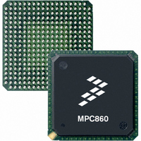
MC68360VR25VL Freescale Semiconductor, MC68360VR25VL Datasheet - Page 525

MC68360VR25VL
Manufacturer Part Number
MC68360VR25VL
Description
IC MPU QUICC 25MHZ 357-PBGA
Manufacturer
Freescale Semiconductor
Datasheets
1.MC68EN360VR25L.pdf
(14 pages)
2.MC68EN360VR25L.pdf
(2 pages)
3.MC68360AI25L.pdf
(962 pages)
Specifications of MC68360VR25VL
Processor Type
M683xx 32-Bit
Speed
25MHz
Voltage
3.3V
Mounting Type
Surface Mount
Package / Case
357-PBGA
Family Name
M68000
Device Core
ColdFire
Device Core Size
32b
Frequency (max)
25MHz
Instruction Set Architecture
RISC
Operating Supply Voltage (max)
3.3V
Operating Supply Voltage (min)
2.7V
Operating Temp Range
0C to 70C
Operating Temperature Classification
Commercial
Mounting
Surface Mount
Pin Count
357
Package Type
BGA
Lead Free Status / RoHS Status
Lead free / RoHS Compliant
Features
-
Lead Free Status / Rohs Status
Compliant
Available stocks
Company
Part Number
Manufacturer
Quantity
Price
Company:
Part Number:
MC68360VR25VL
Manufacturer:
Exar
Quantity:
160
Company:
Part Number:
MC68360VR25VL
Manufacturer:
Freescale Semiconductor
Quantity:
10 000
Company:
Part Number:
MC68360VR25VLR2
Manufacturer:
Freescale Semiconductor
Quantity:
10 000
- Current page: 525 of 962
- Download datasheet (4Mb)
The physical layer of the BISYNC communications link must provide a means of synchro-
nizing the receiver and transmitter. This is usually accomplished by sending at least one pair
of synchronization characters prior to every frame
BISYNC is unusual in that a transmit underrun need not be an error. If an underrun occurs,
the synchronization pattern is transmitted until data is once again ready to transmit. The
receiver discards the additional synchronization characters as they are received. In non-
transparent operation, all synchronization characters (SYNCs) are discarded. In transparent
operation, all DLE-SYNC pairs are discarded. (Correct operation in this case assumes that,
on the transmit side, the underrun does not occur between the DLE and its following char-
acter, a failure mode that is prevented in the QUICC.)
By appropriately setting the SCC mode register, any of the SCC channels may be config-
ured to function as a BISYNC controller. The BISYNC controller handles the basic functions
of the BISYNC protocol in normal mode and in transparent mode.
The SCC in BISYNC mode can work with the TSA or NMSI. The SCC can support modem
lines by a connection to the port C pins or by using the general-purpose I/O pins.
The BISYNC controller consists of separate transmit and receive sections whose operations
are asynchronous with the CPU32+ core and may be either synchronous or asynchronous
with respect to the other SCCs.
7.10.20.1 BISYNC CONTROLLER FEATURES. The BISYNC controller contains the fol-
lowing key features:
7.10.20.2 BISYNC CHANNEL FRAME TRANSMISSION. The
designed to work with almost no intervention from the CPU32+ core. When this CPU32+
core enables the BISYNC transmitter, it will start transmitting SYN1–SYN2 pairs (located in
the data synchronization register) or idle as programmed in the BISYNC mode register. The
BISYNC controller polls the first BD in the transmit channel’s BD table. If there is a message
• Flexible Data Buffers
• Eight Control Character Recognition Registers
• Automatic SYNC1–SYNC2 Detection
• 16-Bit Pattern (BISYNC)
• 8-Bit Pattern (Monosync)
• 4-Bit Pattern (Nibblesync)
• External Sync Pin Support
• SYNC/DLE Stripping and Insertion
• CRC16 and LRC Generation/Checking
• Parity (VRC) Generation/Checking
• Supports BISYNC Transparent Operation (Use of DLE Characters)
• Maintains Parity Error Counter
• Reverse Data Mode
Freescale Semiconductor, Inc.
For More Information On This Product,
MC68360 USER’S MANUAL
Go to: www.freescale.com
Serial Communication Controllers (SCCs)
BISYNC
transmitter
is
Related parts for MC68360VR25VL
Image
Part Number
Description
Manufacturer
Datasheet
Request
R
Part Number:
Description:
Manufacturer:
Freescale Semiconductor, Inc
Datasheet:

Part Number:
Description:
MC68360 MC68360 Multiple Ethernet Channels on the QUICC
Manufacturer:
Motorola / Freescale Semiconductor

Part Number:
Description:
MC68360 Implementing an 8 bit Eprom for an MC68EC040-MC68360 System
Manufacturer:
Motorola / Freescale Semiconductor

Part Number:
Description:
MC68360 Interfacing the MC68060 to the MC68360
Manufacturer:
Motorola / Freescale Semiconductor

Part Number:
Description:
MC68360 MC68360 RAM Microcode Package Option Overview
Manufacturer:
Motorola / Freescale Semiconductor

Part Number:
Description:
MC68360 MC68360 CPM-CPU Interaction
Manufacturer:
Motorola / Freescale Semiconductor

Part Number:
Description:
MC68360 Interfacing SDRAM to the MC68360 QUICC Device
Manufacturer:
Motorola / Freescale Semiconductor

Part Number:
Description:
MC68360 Interfacing the QUICC to a MCM516400 (4Mx4 10-12 column-row) DRAM
Manufacturer:
Motorola / Freescale Semiconductor

Part Number:
Description:
MC68360 Interfacing the 68360 (QUICC) to T1-E1 Systems
Manufacturer:
Motorola / Freescale Semiconductor

Part Number:
Description:
MC68360 Multiple QUICC Design Concept
Manufacturer:
Motorola / Freescale Semiconductor
Part Number:
Description:
Manufacturer:
Freescale Semiconductor, Inc
Datasheet:
Part Number:
Description:
Manufacturer:
Freescale Semiconductor, Inc
Datasheet:
Part Number:
Description:
Manufacturer:
Freescale Semiconductor, Inc
Datasheet:
Part Number:
Description:
Manufacturer:
Freescale Semiconductor, Inc
Datasheet:
Part Number:
Description:
Manufacturer:
Freescale Semiconductor, Inc
Datasheet:


