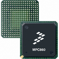
MC68360VR25VL Freescale Semiconductor, MC68360VR25VL Datasheet - Page 309

MC68360VR25VL
Manufacturer Part Number
MC68360VR25VL
Description
IC MPU QUICC 25MHZ 357-PBGA
Manufacturer
Freescale Semiconductor
Datasheets
1.MC68EN360VR25L.pdf
(14 pages)
2.MC68EN360VR25L.pdf
(2 pages)
3.MC68360AI25L.pdf
(962 pages)
Specifications of MC68360VR25VL
Processor Type
M683xx 32-Bit
Speed
25MHz
Voltage
3.3V
Mounting Type
Surface Mount
Package / Case
357-PBGA
Family Name
M68000
Device Core
ColdFire
Device Core Size
32b
Frequency (max)
25MHz
Instruction Set Architecture
RISC
Operating Supply Voltage (max)
3.3V
Operating Supply Voltage (min)
2.7V
Operating Temp Range
0C to 70C
Operating Temperature Classification
Commercial
Mounting
Surface Mount
Pin Count
357
Package Type
BGA
Lead Free Status / RoHS Status
Lead free / RoHS Compliant
Features
-
Lead Free Status / Rohs Status
Compliant
Available stocks
Company
Part Number
Manufacturer
Quantity
Price
Company:
Part Number:
MC68360VR25VL
Manufacturer:
Exar
Quantity:
160
Company:
Part Number:
MC68360VR25VL
Manufacturer:
Freescale Semiconductor
Quantity:
10 000
Company:
Part Number:
MC68360VR25VLR2
Manufacturer:
Freescale Semiconductor
Quantity:
10 000
- Current page: 309 of 962
- Download datasheet (4Mb)
The following bits are used for DRAM bank properties:
PGS2–PGS0—Page Size
DPS1–DPS0—DRAM Port Size
This attribute determines the page size for the DRAM controller (see Table 6-9). The page
size is the smallest DRAM size the user needs to support with page mode capability.
For instance, PGS = 001 (256K) should be used for a 32-bit-wide memory composed of
four 256K
teen 256K
This attribute determines the DRAM bank port size (see Table 6-10). The DRAM controller
asserts the appropriate DSACKx lines according to these bits. If an MC68EC040 access
is performed using this DRAM bank and SPS = 00 or 01, the DRAM controller operates
the same way, but asserts TA instead of DSACK.
The internal DRAM address multiplexer and the page logic sup-
port only a port size of 32 bits or 16 bits. An 8-bit DRAM port size
is not allowed.
The DRAM controller does not support an external DSACKx re-
sponse for a bank on which page mode is used. Also, an exter-
nal DSACK response may not occur before RAS is asserted.
PGS2-PGS0
8 devices, a 16-bit-wide memory composed of two 256K
1 devices. In all cases, the width of the DRAMs is irrelevant.
000
001
010
011
100
101
110
110
Freescale Semiconductor, Inc.
For More Information On This Product,
A11-25(32), A10-25(16)
A11-25(32), A10-25(16)
A12-25(32), A11-25(16)
A12-25(32), A11-25(16)
A13-25(32), A12-25(16)
A13-25(32), A12-25(16)
A14-25(32), A13-25(16)
A10-25(32), A9-25(16)
Address Lines Used
DPS1–DPS0
Table 6-10. DRAM Port Size
Table 6-9. DRAM Page Size
MC68360 USER’S MANUAL
00
01
10
11
Go to: www.freescale.com
NOTES
DRAM Port Size Is 32 Bits
DRAM Port Size Is 16 Bits
External DSACKx Support
Reserved
# Address/Page in Page Compare
Result
1024 Addresses
1024 Addresses
2048 Addresses
2048 Addresses
4096 Addresses
256 Addresses
512 Addresses
512 Addresses
System Integration Module (SIM60)
8 devices, or six-
Related parts for MC68360VR25VL
Image
Part Number
Description
Manufacturer
Datasheet
Request
R
Part Number:
Description:
Manufacturer:
Freescale Semiconductor, Inc
Datasheet:

Part Number:
Description:
MC68360 MC68360 Multiple Ethernet Channels on the QUICC
Manufacturer:
Motorola / Freescale Semiconductor

Part Number:
Description:
MC68360 Implementing an 8 bit Eprom for an MC68EC040-MC68360 System
Manufacturer:
Motorola / Freescale Semiconductor

Part Number:
Description:
MC68360 Interfacing the MC68060 to the MC68360
Manufacturer:
Motorola / Freescale Semiconductor

Part Number:
Description:
MC68360 MC68360 RAM Microcode Package Option Overview
Manufacturer:
Motorola / Freescale Semiconductor

Part Number:
Description:
MC68360 MC68360 CPM-CPU Interaction
Manufacturer:
Motorola / Freescale Semiconductor

Part Number:
Description:
MC68360 Interfacing SDRAM to the MC68360 QUICC Device
Manufacturer:
Motorola / Freescale Semiconductor

Part Number:
Description:
MC68360 Interfacing the QUICC to a MCM516400 (4Mx4 10-12 column-row) DRAM
Manufacturer:
Motorola / Freescale Semiconductor

Part Number:
Description:
MC68360 Interfacing the 68360 (QUICC) to T1-E1 Systems
Manufacturer:
Motorola / Freescale Semiconductor

Part Number:
Description:
MC68360 Multiple QUICC Design Concept
Manufacturer:
Motorola / Freescale Semiconductor
Part Number:
Description:
Manufacturer:
Freescale Semiconductor, Inc
Datasheet:
Part Number:
Description:
Manufacturer:
Freescale Semiconductor, Inc
Datasheet:
Part Number:
Description:
Manufacturer:
Freescale Semiconductor, Inc
Datasheet:
Part Number:
Description:
Manufacturer:
Freescale Semiconductor, Inc
Datasheet:
Part Number:
Description:
Manufacturer:
Freescale Semiconductor, Inc
Datasheet:


