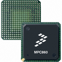
MC68360VR25VL Freescale Semiconductor, MC68360VR25VL Datasheet - Page 718

MC68360VR25VL
Manufacturer Part Number
MC68360VR25VL
Description
IC MPU QUICC 25MHZ 357-PBGA
Manufacturer
Freescale Semiconductor
Datasheets
1.MC68EN360VR25L.pdf
(14 pages)
2.MC68EN360VR25L.pdf
(2 pages)
3.MC68360AI25L.pdf
(962 pages)
Specifications of MC68360VR25VL
Processor Type
M683xx 32-Bit
Speed
25MHz
Voltage
3.3V
Mounting Type
Surface Mount
Package / Case
357-PBGA
Family Name
M68000
Device Core
ColdFire
Device Core Size
32b
Frequency (max)
25MHz
Instruction Set Architecture
RISC
Operating Supply Voltage (max)
3.3V
Operating Supply Voltage (min)
2.7V
Operating Temp Range
0C to 70C
Operating Temperature Classification
Commercial
Mounting
Surface Mount
Pin Count
357
Package Type
BGA
Lead Free Status / RoHS Status
Lead free / RoHS Compliant
Features
-
Lead Free Status / Rohs Status
Compliant
Available stocks
Company
Part Number
Manufacturer
Quantity
Price
Company:
Part Number:
MC68360VR25VL
Manufacturer:
Exar
Quantity:
160
Company:
Part Number:
MC68360VR25VL
Manufacturer:
Freescale Semiconductor
Quantity:
10 000
Company:
Part Number:
MC68360VR25VLR2
Manufacturer:
Freescale Semiconductor
Quantity:
10 000
- Current page: 718 of 962
- Download datasheet (4Mb)
Scan Chain Test Access Port
8.4 INSTRUCTION REGISTER
The QUICC JTAG implementation includes the public instructions (EXTEST, SAMPLE/
PRELOAD, and BYPASS), and also supports the CLAMP instruction. One additional public
instruction (HI-Z) provides the capability for disabling all device output drivers. The QUICC
includes a 3-bit instruction register without parity consisting of a shift register with three par-
allel outputs. Data is transferred from the shift register to the parallel outputs during the
update-IR controller state. The three bits are used to decode the five unique instructions
listed in Table 8-3.
The parallel output of the instruction register is reset to all ones in the test-logic-reset con-
troller state. Note that this preset state is equivalent to the BYPASS instruction.
During the capture-IR controller state, the parallel inputs to the instruction shift register are
loaded with the CLAMP command code.
8.4.1 EXTEST
The external test (EXTEST) instruction selects the 196-bit boundary scan register. EXTEST
also asserts internal reset for the QUICC system logic to force a predictable benign internal
state while performing external boundary scan operations.
By using the TAP, the register is capable of a) scanning user-defined values into the output
buffers, b) capturing values presented to input pins, c) controlling the direction of bidirec-
tional pins, and d) controlling the output drive of three-stateable output pins. For more details
on the function and use of EXTEST, refer to the scan chaindocument.
8.4.2 SAMPLE/PRELOAD
The SAMPLE/PRELOAD instruction initializes the boundary scan register output cells prior
to selection of EXTEST. This initialization ensures that known data will appear on the out-
puts when entering the EXTEST instruction. The SAMPLE/PRELOAD instruction also pro-
vides a means to obtain a snapshot of system data and control signals. In the case of the
QUICC, this functionality is not supported.
8-10
Since there is no internal synchronization between the scan
chain clock (TCK) and the system clock (CLKO1), the user must
Freescale Semiconductor, Inc.
For More Information On This Product,
Table 8-3. Instruction Decoding
B2
0
0
X
1
1
MC68360 USER’S MANUAL
Code
Go to: www.freescale.com
B1
0
0
1
0
0
B0
NOTE
X
0
1
0
1
CLAMP and BYPASS
SAMPLE/PRELOAD
Instruction
BYPASS
EXTEST
HI-Z
Related parts for MC68360VR25VL
Image
Part Number
Description
Manufacturer
Datasheet
Request
R
Part Number:
Description:
Manufacturer:
Freescale Semiconductor, Inc
Datasheet:

Part Number:
Description:
MC68360 MC68360 Multiple Ethernet Channels on the QUICC
Manufacturer:
Motorola / Freescale Semiconductor

Part Number:
Description:
MC68360 Implementing an 8 bit Eprom for an MC68EC040-MC68360 System
Manufacturer:
Motorola / Freescale Semiconductor

Part Number:
Description:
MC68360 Interfacing the MC68060 to the MC68360
Manufacturer:
Motorola / Freescale Semiconductor

Part Number:
Description:
MC68360 MC68360 RAM Microcode Package Option Overview
Manufacturer:
Motorola / Freescale Semiconductor

Part Number:
Description:
MC68360 MC68360 CPM-CPU Interaction
Manufacturer:
Motorola / Freescale Semiconductor

Part Number:
Description:
MC68360 Interfacing SDRAM to the MC68360 QUICC Device
Manufacturer:
Motorola / Freescale Semiconductor

Part Number:
Description:
MC68360 Interfacing the QUICC to a MCM516400 (4Mx4 10-12 column-row) DRAM
Manufacturer:
Motorola / Freescale Semiconductor

Part Number:
Description:
MC68360 Interfacing the 68360 (QUICC) to T1-E1 Systems
Manufacturer:
Motorola / Freescale Semiconductor

Part Number:
Description:
MC68360 Multiple QUICC Design Concept
Manufacturer:
Motorola / Freescale Semiconductor
Part Number:
Description:
Manufacturer:
Freescale Semiconductor, Inc
Datasheet:
Part Number:
Description:
Manufacturer:
Freescale Semiconductor, Inc
Datasheet:
Part Number:
Description:
Manufacturer:
Freescale Semiconductor, Inc
Datasheet:
Part Number:
Description:
Manufacturer:
Freescale Semiconductor, Inc
Datasheet:
Part Number:
Description:
Manufacturer:
Freescale Semiconductor, Inc
Datasheet:


