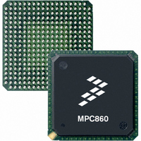
MC68360VR25VL Freescale Semiconductor, MC68360VR25VL Datasheet - Page 721

MC68360VR25VL
Manufacturer Part Number
MC68360VR25VL
Description
IC MPU QUICC 25MHZ 357-PBGA
Manufacturer
Freescale Semiconductor
Datasheets
1.MC68EN360VR25L.pdf
(14 pages)
2.MC68EN360VR25L.pdf
(2 pages)
3.MC68360AI25L.pdf
(962 pages)
Specifications of MC68360VR25VL
Processor Type
M683xx 32-Bit
Speed
25MHz
Voltage
3.3V
Mounting Type
Surface Mount
Package / Case
357-PBGA
Family Name
M68000
Device Core
ColdFire
Device Core Size
32b
Frequency (max)
25MHz
Instruction Set Architecture
RISC
Operating Supply Voltage (max)
3.3V
Operating Supply Voltage (min)
2.7V
Operating Temp Range
0C to 70C
Operating Temperature Classification
Commercial
Mounting
Surface Mount
Pin Count
357
Package Type
BGA
Lead Free Status / RoHS Status
Lead free / RoHS Compliant
Features
-
Lead Free Status / Rohs Status
Compliant
Available stocks
Company
Part Number
Manufacturer
Quantity
Price
Company:
Part Number:
MC68360VR25VL
Manufacturer:
Exar
Quantity:
160
Company:
Part Number:
MC68360VR25VL
Manufacturer:
Freescale Semiconductor
Quantity:
10 000
Company:
Part Number:
MC68360VR25VLR2
Manufacturer:
Freescale Semiconductor
Quantity:
10 000
- Current page: 721 of 962
- Download datasheet (4Mb)
Freescale Semiconductor, Inc.
SECTION 9
APPLICATIONS
9.1 MINIMUM SYSTEM CONFIGURATION
This section describes a basic minimum system configuration for the QUICC. It discusses
the hardware and software issues of configurating the QUICC to support a basic system with
a variety of ROM and RAM types.
9.1.1 QUICC Hardware Configuration
These paragraphs discuss the hardware issues relating to the configuration of the QUICC.
Reference Figure 9-1 during these discussions. This configuration assumes a 32-bit data
bus. Comments about the changes required for a 16-bit data bus solution are given at the
end of the discussion.
9.1.1.1 QUICC BASIC ACCESSES. The basic connection is made through the data and
address bus. All 32 data lines are used in this application, although not all memories are a
full 32-bits wide.
Twenty-eight address lines are used, giving a 256-Mbytes address capability. It is possible
to use all 32 address lines, but the QUICC would then lose its write enable lines (WE3–
WE0). Since these lines are very useful in memory interfaces, they are used in the applica-
tion.
The function code (FC3–FC0) and data strobe (DS) lines are shown routed to the system
bus, although the memories in this application do not require them.
Other pins not directly needed are DSACKx, BERR, SIZx, PERR, IPIPEx, and a number of
chip selects. The DSACKx lines are not required because the on-chip wait state generator
is used. The BERR pin is not needed because all bus errors are generated by internal mon-
itor logic. The SIZx pins are not needed because the memory controller has programmable
port sizes for each memory bank. The PERR pin is not needed because parity errors gen-
erate bus errors. The IPIPEx pins are only needed for emulator support. The additional chip
selects can be used to add additional peripherals as required.
MC68360 USER’S MANUAL
For More Information On This Product,
Go to: www.freescale.com
Related parts for MC68360VR25VL
Image
Part Number
Description
Manufacturer
Datasheet
Request
R
Part Number:
Description:
Manufacturer:
Freescale Semiconductor, Inc
Datasheet:

Part Number:
Description:
MC68360 MC68360 Multiple Ethernet Channels on the QUICC
Manufacturer:
Motorola / Freescale Semiconductor

Part Number:
Description:
MC68360 Implementing an 8 bit Eprom for an MC68EC040-MC68360 System
Manufacturer:
Motorola / Freescale Semiconductor

Part Number:
Description:
MC68360 Interfacing the MC68060 to the MC68360
Manufacturer:
Motorola / Freescale Semiconductor

Part Number:
Description:
MC68360 MC68360 RAM Microcode Package Option Overview
Manufacturer:
Motorola / Freescale Semiconductor

Part Number:
Description:
MC68360 MC68360 CPM-CPU Interaction
Manufacturer:
Motorola / Freescale Semiconductor

Part Number:
Description:
MC68360 Interfacing SDRAM to the MC68360 QUICC Device
Manufacturer:
Motorola / Freescale Semiconductor

Part Number:
Description:
MC68360 Interfacing the QUICC to a MCM516400 (4Mx4 10-12 column-row) DRAM
Manufacturer:
Motorola / Freescale Semiconductor

Part Number:
Description:
MC68360 Interfacing the 68360 (QUICC) to T1-E1 Systems
Manufacturer:
Motorola / Freescale Semiconductor

Part Number:
Description:
MC68360 Multiple QUICC Design Concept
Manufacturer:
Motorola / Freescale Semiconductor
Part Number:
Description:
Manufacturer:
Freescale Semiconductor, Inc
Datasheet:
Part Number:
Description:
Manufacturer:
Freescale Semiconductor, Inc
Datasheet:
Part Number:
Description:
Manufacturer:
Freescale Semiconductor, Inc
Datasheet:
Part Number:
Description:
Manufacturer:
Freescale Semiconductor, Inc
Datasheet:
Part Number:
Description:
Manufacturer:
Freescale Semiconductor, Inc
Datasheet:


