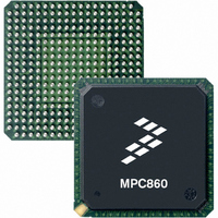
MC68360VR25VL Freescale Semiconductor, MC68360VR25VL Datasheet - Page 732

MC68360VR25VL
Manufacturer Part Number
MC68360VR25VL
Description
IC MPU QUICC 25MHZ 357-PBGA
Manufacturer
Freescale Semiconductor
Datasheets
1.MC68EN360VR25L.pdf
(14 pages)
2.MC68EN360VR25L.pdf
(2 pages)
3.MC68360AI25L.pdf
(962 pages)
Specifications of MC68360VR25VL
Processor Type
M683xx 32-Bit
Speed
25MHz
Voltage
3.3V
Mounting Type
Surface Mount
Package / Case
357-PBGA
Family Name
M68000
Device Core
ColdFire
Device Core Size
32b
Frequency (max)
25MHz
Instruction Set Architecture
RISC
Operating Supply Voltage (max)
3.3V
Operating Supply Voltage (min)
2.7V
Operating Temp Range
0C to 70C
Operating Temperature Classification
Commercial
Mounting
Surface Mount
Pin Count
357
Package Type
BGA
Lead Free Status / RoHS Status
Lead free / RoHS Compliant
Features
-
Lead Free Status / Rohs Status
Compliant
Available stocks
Company
Part Number
Manufacturer
Quantity
Price
Company:
Part Number:
MC68360VR25VL
Manufacturer:
Exar
Quantity:
160
Company:
Part Number:
MC68360VR25VL
Manufacturer:
Freescale Semiconductor
Quantity:
10 000
Company:
Part Number:
MC68360VR25VLR2
Manufacturer:
Freescale Semiconductor
Quantity:
10 000
- Current page: 732 of 962
- Download datasheet (4Mb)
Applications
The memory controller status register (MSTAT) is used for reporting parity errors and does
not require initialization.
The eight base registers (BRs), one for each memory bank, should be configured as follows:
The eight option registers (ORs), one for each memory bank, should be configured as fol-
lows:
9.1.3.3 USING THE QUICC IN 16-BIT DATA BUS MODE. For systems that do not require
a full 32-bit data bus capability, the QUICC offers a 16-bit data bus mode. A system with 16-
bit data bus mode is almost the same as the system shown in this section. Only a few
changes are required.
9-12
NCS should normally be cleared.
DWQ depends on timing. It must be set if page mode is used for the DRAMs.
DW40 is not used and should be cleared.
AMUX should be set.
The BA31–BA11 bits may be set as desired. Different memory arrays should not overlap.
For simplicity, FC3–FC0 can be cleared.
TRLXQ should normally be cleared for memory interfaces.
BACK40 is not used and should be cleared.
CSNT40 is not used and should be cleared.
CSNTQ should normally be cleared.
PAREN should be set for memory banks that use parity.
WP should be set for EPROM, burst EPROM, and flash EPROM; otherwise, it should be
cleared.
V should be set if the memory bank is used.
The TCYC bits should be set to determine the number of wait states required.
The AM27–AM11 bits should be programmed to determine the block size of the chip se-
lect or RASx line. This should be the total number of bytes in each memory array.
FCM3–FCM0 may be set to all zeros to allow the chip select or RASx line to assert on all
function codes except CPU space (interrupt acknowledge). It is advisable to program
FCM3–FCM0 to zeros, at least during the initial stages of debugging.
BCYC1–BCYC0 are not used and should be cleared.
PGME may be set as desired to enable page mode if this is a DRAM bank.
SPS1–SPS0 should be set to 10 for the byte-wide memory banks, such as EPROM, and
cleared for the 32-bit-wide memory banks.
DSSEL should be set only if this is a DRAM bank.
Freescale Semiconductor, Inc.
For More Information On This Product,
MC68360 USER’S MANUAL
Go to: www.freescale.com
Related parts for MC68360VR25VL
Image
Part Number
Description
Manufacturer
Datasheet
Request
R
Part Number:
Description:
Manufacturer:
Freescale Semiconductor, Inc
Datasheet:

Part Number:
Description:
MC68360 MC68360 Multiple Ethernet Channels on the QUICC
Manufacturer:
Motorola / Freescale Semiconductor

Part Number:
Description:
MC68360 Implementing an 8 bit Eprom for an MC68EC040-MC68360 System
Manufacturer:
Motorola / Freescale Semiconductor

Part Number:
Description:
MC68360 Interfacing the MC68060 to the MC68360
Manufacturer:
Motorola / Freescale Semiconductor

Part Number:
Description:
MC68360 MC68360 RAM Microcode Package Option Overview
Manufacturer:
Motorola / Freescale Semiconductor

Part Number:
Description:
MC68360 MC68360 CPM-CPU Interaction
Manufacturer:
Motorola / Freescale Semiconductor

Part Number:
Description:
MC68360 Interfacing SDRAM to the MC68360 QUICC Device
Manufacturer:
Motorola / Freescale Semiconductor

Part Number:
Description:
MC68360 Interfacing the QUICC to a MCM516400 (4Mx4 10-12 column-row) DRAM
Manufacturer:
Motorola / Freescale Semiconductor

Part Number:
Description:
MC68360 Interfacing the 68360 (QUICC) to T1-E1 Systems
Manufacturer:
Motorola / Freescale Semiconductor

Part Number:
Description:
MC68360 Multiple QUICC Design Concept
Manufacturer:
Motorola / Freescale Semiconductor
Part Number:
Description:
Manufacturer:
Freescale Semiconductor, Inc
Datasheet:
Part Number:
Description:
Manufacturer:
Freescale Semiconductor, Inc
Datasheet:
Part Number:
Description:
Manufacturer:
Freescale Semiconductor, Inc
Datasheet:
Part Number:
Description:
Manufacturer:
Freescale Semiconductor, Inc
Datasheet:
Part Number:
Description:
Manufacturer:
Freescale Semiconductor, Inc
Datasheet:


